1. Introduction
The performance of GaN-based devices is significantly influenced by the quality of the metallic contacts used to make connection to power sources and/or other devices [1]. The electrical properties of metal/n-GaN contacts depend on a wide variety of processing parameters, such as cleaning and etching of the GaN surface [2, 3], the composition and thickness of the metallic contacting layers, and the annealing temperature and atmosphere used to activate the contact. Because enhanced diffusion couple metallization layers and annealing conditions have been identified to gain improved contact performance, increased attention is also being given to the preparation of GaN surfaces prior to metallization. For example, previous work has shown that ohmic contacts of lower resistance can be obtained by making contact to plasma or wet-etched surfaces [4].
Detailed investigations are required to appraise the intimate relationship between the chemical treatment employed, the resulting chemical/structural modifications to the GaN surface and the electrical properties of the contacts. Whilst detailed understanding has been gained on the effects of surface cleaning, for example HCl [5] or HF [6] treatments, much less is known about the consequences of surface etching, for example KOH or plasma treatments, partly because of the dual action of the removal of GaN material combined with surface cleaning. One approach to address this problem is to compare cleaned and etched surfaces in order to assess the consequences of the removal of GaN material on contact performance. Furthermore, in order to appraise the effects of GaN surface treatment on the performance of electrical contacts, it is helpful to use metallic contacts that do not alloy with GaN, such as Au [7] or Pt [8], thus avoiding further modification to the GaN material.
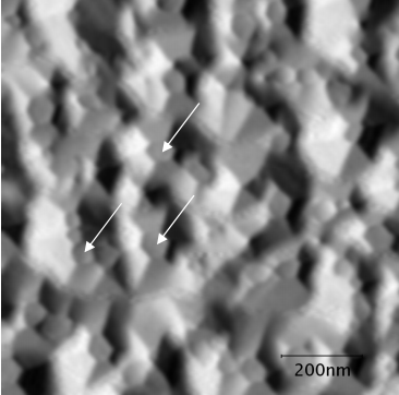
The present work studies the mechanisms that determine the barrier height by investigating the effects of KOH etching on the properties of n-GaN surfaces and associated Au/n-GaN Schottky contacts. To investigate the role of KOH etching beyond surface cleaning, the KOH treatment was used in conjunction with an HCl clean (samples denoted as 'KOH treated') and compared with a reference HCl clean (samples denoted as 'reference'). Hence, reference and KOH-treated n-GaN surfaces have been investigated, initially with regard to sample surface composition, bonding states, morphology and crystalline structure. Consideration has then given to the electrical properties of Au Schottky contacts deposited onto these treated n-GaN surfaces, in order to appraise the respective electron barrier heights and the extent of non-radiative recombination activity. In this context, surfaces of Ga-polar GaN/sapphire grown by molecular beam epitaxy (MBE) and metal-organic chemical vapour deposition (MOCVD) are also compared.
2. Experimental
The starting MBE GaN/sapphire wafer was 2.5 µm thick and exhibited an n-type carrier concentration of 6.4 x 1016 cm.-3 The MOCVD GaN/sapphire (0001) wafer was 3 µm thick with a 0.9 µm thick Sidoped capping layer and an estimated n-type carrier concentration of 1 x 1017 cm.-3 Cleaved samples were first sequentially degreased using a standard procedure of ultrasonic baths of lotoxane, methanol, acetone, propanol and de-ionized water, for three minutes each. The subsequent KOH treatment consisted of sample dipping in a 4 molar solution of KOH and de-ionized water for 1 minute at 60ºC, followed by a 1 minute dip in de-ionized water, then blowing dry using N2. The cleaning process consisted of dipping into a 37 % solution of HCl and de-ionised water for three minutes, again blowing dry using N2. The surface chemistry of the etched GaN samples was appraised by X-ray photoelectron spectroscopy (XPS) using a VG scientific ESCALAB spectrometer using AlKα X-rays at an anode voltage of 10 kV and a filament emission current of 20 mA. Samples were loaded into the XPS chamber immediately after the final HCl cleaning stage. Surface morphology was investigated by atomic force microscopy (AFM) using a Dimension AFM in tapping mode. The near-surface crystallographic structure of samples was assessed by means of reflection high-energy-electron diffraction (RHEED), performed within a modified Jeol 2000fx transmission electron microscope (TEM), using the glancing-angle diffraction of electrons at the surface of specimens mounted vertically just below the projector lens.
3. Results
3.1. Characterization of n-GaN surfaces
The acquired XPS survey spectra covering the 0-1100 eV binding energy range were dominated by N and Ga peaks, with significant levels of C and traces of O and Cl, in all cases. The atomic weight percentages (atom wt %) of the surface species were determined using peak areas and sensitivity factors appropriate for N1s, Ga3d, C1s, O1s and Cl2p photoelectron lines, as summarized in Table 1. These elemental ratios are comparative and do not represent absolute stoichiometry since the photoionization cross-section and transmission function of the spectrometer for each element are not taken into account. However, a distinct trend is revealed, with the KOH treatment resulting in an increase of the N surface content and a decrease of the Ga surface content for the case of both MBE and MOCVD samples, in agreement with [9] for the case of MOCVD-grown GaN. It is also evident, following KOH treatment, that the surface C content decreased slightly for the case of the MBE-grown GaN and significantly for the case of the MOCVD-grown sample. Variations in the O and Cl surface content were also detected, but these values were below 1 %, and on the scale of the sensitivity of this XPS experimental arrangement. No remnant K content was detected as a consequence of the KOH treatment.

Fig1
4. Discussion
The combined AFM, SE and RHEED investigations provide a clear description of the sample surface morphology and near-surface microstructure, whilst I-V and EBIC characterization provide evidence for changes in the contact electronic barrier height and the level of non-radiative recombination as a consequence of KOH treatment. Furthermore, XPS data provide clues to changes in the surface chemistry and by implication surface electronic structure, following etching, to help reconcile these observations.
上一篇: 通过旋涂在单晶硅晶片上形成发射极层
下一篇: 碳酸氢钠溶液氧化单晶硅太阳能电池的研究