1. Introduction
Over the last decades, nanocrystalline semiconductors have been widely studied, due to their physical properties relative to those of bulk crystals. The high surface area, band gap shift, and effificient luminescence have made the use of porous semiconductor over a promising material for a wide range of applications; from optoelectronics to chemical and biochemical sensors [1,2]. Recently, many works [3–9] have been directed towards depositing semiconductor layers on porous substrates, because of the demand for more powerful and sophisticated device applications. One of the reasons for using a porous semiconductor as a substrate for depositing semiconductor layers is that the nano-patterned porous structures can reduce the extended defect density [6]. The interest in porous semiconductor arises from the fact that they can act as a sink for threading dislocations and accommodate the strain. Hence, they are widely used as a buffer or intermediate layer in epitaxial growth to obtain a subsequent layer with less strain and dislocation densities [10,11]. Mynbaeva et al. [12] proposed that the growth of GaN on porous GaN could lead to high-quality strain-released epilayers.
One of the main factors that affect the electrochemical etching is the electrolyte. Many electrolytes were reported for etching semiconductors. HF-based solutions are the most utilized solutions for GaAs, SiC, and GaN porosifification [21]. The electrolytes based on H2SO4 or H3PO4 acids are more preferable for GaP porosifification, because they allow the attainment of porous structures without visible covering of pore surface by oxides or other reaction products [16]. For InP, better results were obtained in KOH and HCl-based solutions [15]. Due to their different chemical nature, wide ranges of aqueous electrolytes have been used for GaN etching. Many works in photoelectrochemical etching of GaN were done in alkaline aqueous solutions containing inorganic KOH [20,22], and in inorganic acids such as H2SO4 [23], and H3PO4 [24] or into halogen acids such as HF and HCl [25]. In addition, the morphology is strongly dependent on the chemical nature of the solvent, the concentration of the conduction salt, the pH, the counter ion and the temperature [26]. Thus, it is very important to investigate the suitable electrolyte for GaN [27].
2. Experimental procedure
The samples used in this study were commercial n-GaN grown by metalorganic chemical vapor deposition (MOCVD) on Al2O3 substrates. The electron concentration (Si doped) obtained by Hall measurements was n = 1 × 1017 cm−3. The samples were cleaned fifirst with acetone and methanol, then in 1:20 NH4OH:H2O for 10 min, followed by a third cleaning in 1:50 HF:H2O solution to remove the surface oxides. This was followed by a fourth cleaning in 3:1 HCl:HNO3 at 80 ◦C for 10 min. Between the cleaning steps, the samples were rinsed in deionized water. Aluminum was then partly evaporated at a corner of the surface of GaN sample using a thermal evaporation system under a pressure of 3.4 × 10⁻⁵ Torr. Al was used since it provides an ohmic contact [28]. By using a homemade Teflflon cell, we fifixed the GaN sample as an anode and Pt wire as a cathode.
We used four different solutions to produce porous GaN. The fifirst electrolyte was a mixture of aqueous HF solution and absolute ethanol C2H5OH (1:4) by volume with pH of 4.3. The second electrolyte was a mixture of HF solution and nitric acid HNO3 (1:4) with pH of 1.66. The third solution was potassium hydroxide KOH with pH of 14, and the fourth electrolyte was a mixture of sulphuric acid H2SO4 and H2O2 (3:1) with pH of 4.5. In the electrochemical etching process, we used constant current density of J = 5 mA/cm2 for 20 min (supplied by a Keithley 220 programmable current source) and a low power UV lamp (∼4W). After etching, the samples were rinsed in deionized water and dried in ambient air.
3. Results and discussion
3.1. The mechanism of photoelectrochemical (PEC) etching of GaN
Both holes and OH− ions take active parts in the etching of the GaN. It should be noted that the two-step process described by Eqs. (2) and (3)is essentially equivalent to the overall reaction described by Eq. (1). It has been observed that bubbles are often found near the surface of the sample during PEC etching, which may came from the release of N2. In addition, the photoelectrochemical etching current decreased gradually due to the increasing oxide thickness. During the chemical etching, bond exchange proceeds simultaneously between undissociated molecules and the surface atoms in the solution. Chemical bonds between the surface atoms and the bulk atoms are broken while new bonds are formed between Ga and O2 and move to the soluti.
3.2. Porosity and surface morphology
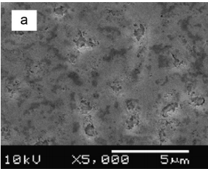
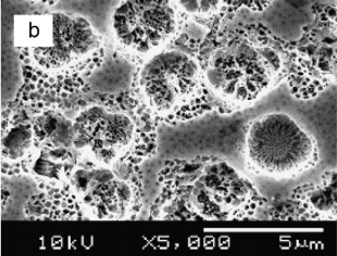
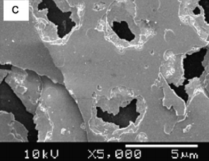
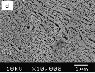
One of the most important characteristics of porous semiconductors layers is their porosity (P), which is defifined as the fraction of void in the porous structure given by [35] P = W1 − W2 W1 − W3 (4) where W1, W2 and W3 denote the weight of the original, anodized, and stripped wafer, respectively. The measured porosities P were 13%, 30%, 42% and 53% of the samples etched in HF:C2H5OH, HF:HNO3, KOH and H2SO4:H2O2 respectively. Thesemeasurements show that the porosity strongly dependent on the electrolytes and thus affecting the surface morphology of the samples as shown in Fig. 1.


Fig1
4. Conclusions
A simple and cost-effective method in UV enhanced electrochemical etching has been applied to Si-doped GaN to produce porous GaN using different electrolytes. All porous GaN showed strong dependence of porosity, surface morphology and optical properties on electrolyte types. In general, the optical properties of the etched samples were improved compared to the as grown sample. The sample etched in H2SO4:H2O2 (3:1) exhibited uniform surface morphology, highest porosity and the highest enhancement of PL emission. Raman spectra of all the porous samples with E2 (high) peak has been observed to be slightly shifted to lower frequency relative to the as-grown sample, suggesting that stress relaxation has taken place in the samples.
上一篇: 晶片键合过程中保持晶片对准精度的方法
下一篇: 多孔GaN的结构和光学特性