1. Introduction
The fabrication of porous semiconductors has attracted a great deal of research interest recently. These materials exhibit unique chemical and physical properties due to their extremely small size and large surface to volume ratio; therefore it offers alternative possibilities for their various potential applications in optoelectronics, chemical and biochemical sensing [1–2].
Recently, considerable effort has been directed towards the synthesis of porous GaN. The research in porous GaN is strongly driven by the superior physical properties such as the excellent thermal, mechanical and chemical stability, as well as the shift of the bandgap [3] and potential applications in chemical sensing [4,5]. Since the report of visible luminescence from porous silicon in 1990 [6], signifificant advances have been made on the studies of the structural, optical as well as mechanical and electrical properties of the porous Si. On the contrary, the study of porous GaN is still in the early stage of development, most of the fundamental properties are not well-documented.
2. Experimental details
The commercial 2-inch diameter GaN wafer (from Technologies and Devices International Inc., USA) was used in this study. This was an unintentionally doped n-type GaN grown on C-plane sapphire substrate. The thickness of GaN fifilm was about 3.0 µm with carrier concentration of ~4.38 × 1017 cm−3 . The wafer was then cleaved into few pieces. Prior to the metallization, the native oxide of the sample was removed in the 1:20 =NH4OH:H2O solution, followed by 1:50 HF: H2O. Subsequently boiling aqua regia (3:1 =HCl:HNO3 ) was used to etch and clean the sample. Porous GaN in this work was generated by Pt assisted electroless etching. Two narrow stripes of Pt with thickness of about 150 nm were deposited on the GaN sample by using sputtering system. The samples were then etched in a solution of 4:1:1 =HF:CH3OH:H2O2 under illumination of an UV lamp with 500 W power for 15, 30, 60 and 90 min, respectively. The morphological, structural and optical properties of porous GaN samples were characterized by scanning electron microscopy (SEM), atomic force microscopy (AFM), Raman scattering and optical transmission (OT).
3. Results and discussions
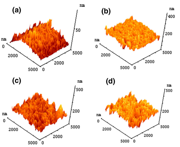
SEM images of the porous GaN samples generated under different durations were shown in Fig. 1. For 15-min sample, the etching was in the initial stage, ridges and valleys were gradually formed, however no pore was found. For 30-min sample, ridges and valleys were formed with pores observed at the valley area. On the other hand, the samples etched for 60 min or longer duration, the surface morphology was found to be similar, suggesting that an etching saturation was reached, at this stage, high density of pores were observed. The etching duration has no signifificant effect on the pores. The size and shape of the pores remained relatively constant for those samples etched for 30, 60 and 90 min. From the SEM images, only circular-shaped pores were observed with the size ranging from 50 to 80 nm and the pore densities for 30, 60 and 90-min etched samples were determined to be 0.7×10¹⁰, 1.1×10¹⁰ and 1.1×1010 cm−2 , respectively.

Fig1
It is interesting to note that porous GaN generated by electroless etching technique does not necessary to have identical morphological evolution. Diaz et al [7,8] prepared the porous GaN samples by Pt assisted electroless etching, in their porous samples, for short etch time (b15 min), a rich network of small pores formed, however for longer etch times, ridge-valley-like morphology would appear. In contrast, no pore formation was observed in our sample for short etching duration (15 min). On the other hand, porous GaN produced by Vajpeyi et al [9] using similar method was found to have different pore shapes and sizes under different etching durations.
上一篇: 不同电解质对多孔氮化镓的影响
下一篇: 反应离子蚀刻的实用方法