Introduction: The development of effective processing methods for GaN and related materials remains an important research effort for practical device realisation. While conventional dry etching techniques have been successfully applied towards etching of the groupIII nitrides [1], very few wet etchants have been identifified. Room temperature etching of AlN has been reported using AZ200K developer [2], while InN fifilms may be etched in aqueous KOH and NaOH at elevated temperatures [3, 4]. GaN has been found to etch only very slowly (~2nm/min) in NH4OH solutions [4]. Since dry etching processes possess a number of signifificant drawbacks compared to wet etching techniques, such as the formation of ion-induced damage, it is important to explore alternative processing methods.
Photoelectrochemical (PEC) etching is a technique in which the photogeneration of electrons and holes in a material enhances chemical etching of the material. Wet PEC etching has been explored for a variety of semiconductor materials and shown to produce high etch rates, good anisotropy, as well as high selectivity between materials of different doping and bandgap [5 – 7]. Minsky et al. [8] have recently demonstrated the feasibility of PEC etching of GaN under illumination by a He-Cd laser (λ = 325nm) using KOH and HCl solutions. They demonstrated high etch rates for non-intentionally doped (NID) GaN (n = 2–4 × 10¹⁷) using annealed (at 900°C) Ti contacts to form the electrical contacts and etch mask. In this Letter, we report on PEC etching of GaN samples of n+, NID, and p-type dopings carried out over large areas using Hg lamp exposure and unannealed, as-deposited Ti metal contacts.
Signifificantly, no appreciable etching was observed for the p-type samples. Previous work on PEC etching of GaAs has established that etch rates are dependent upon confifinement of photogenerated holes to the semiconductor surface [5, 6]. Minsky et al. have suggested that the etching mechanism for GaN may be similar to that proposed for GaAs, in which photogenerated holes participate in the oxidative decomposition of Ga and As [8]. The negligible etch rates observed for p-GaN are consistent with previously reported results for p-GaAs, in which ‘surface band bending’ prevents the accumula-tion of holes at the semiconductor surface and inhibits the oxidation reaction from occurring [5, 6].

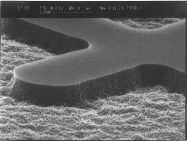
Fig1
These results suggest that the PEC etch process may be very useful for dopant selective etching of GaN layers. Preliminary experiments have been carried out in which a vertical cross-section of the p-n heterostructure was exposed to UV radiation while immersed in solution. Electrical connection was made to the sample through the Ni contact pads on the p-type layer, as described above. Selective etching of the buried n-type layer occurred, producing deep undercutting of the top p-type layer. No etching of the p-type material was observed. Selective PEC etching may be an effective technique for achieving smoothly etched surfaces by use of an etch-stop layer of ptype doping or wider bandgap material. In addition, the ability to produce undercut profifiles can be useful for device fabrication, which is not readily accomplished using dry etching techniques.
NID and n+ GaN samples with dimensions of ~0.5 × 1cm were etched to investigate the uniformity of the process over large areas. For n+ samples, variations in etch depth of ~20–30% were observed over this area, with reduced etching occurring near the sample edges. On the NID samples, etch rates dropped off by as much as 80% for surface regions distanced > ~1.5mm from the electrical contact. Similar variations in etch depth have been previously observed for PEC etching of resistive materials and has been attributed to potential drops across the sample surface [6, 7]. The use of a backside contact to the SiC substrate may help provide more uniform etching on NID layers.
上一篇: 反应离子蚀刻的实用方法
下一篇: GaN、ZnO和SiC的湿法化学蚀刻