There are a number of challenges when processing compound semiconductors, including the relatively high vapor pressures of the group V and VI elements compared to the group III and II elements and the difficulty in forming highly reliable Ohmic and rectifying contacts. It is necessary to develop highly selective, as well as non-selective, etch processes for the different materials in the heterostructure systems available with both GaN (ie. InGaN/GaN/AlGaN) and ZnO (namely ZnMgO/ZnO/ZnCdO). Much effort is devoted to achieving lattice-matched compositions, to avoid the introduction of threading dislocations which degrade the electrical transport and optical qualities of devices subsequently fabricated. To some extent the InGaN/AlGaN system represents an exception, since highly luminescent light emitting diodes (LEDs) and laser diodes have been demonstrated.(2,3) For LEDs the resultant reliability is sufficient for commercial applications, but the high dislocation density in heteroepitaxial material limits the lifetime of laser diodes, where the much higher current density leads to metal migration that shorts out the p-n junction. In material grown on quasi-GaN substrates, this mechanism is absent (4), and the laser diodes have much longer lifetime.
The etch rate may be limited by the diffusion of the active etchant species to the semiconductor surface, or by the diffusion away of the soluble product.(5) In this case the etching is termed diffusion-limited, and its characteristic include a square root dependence of etch depth on etch time, an activation energy ≤6 kCal.mol-1 and a strong dependence of etch rate on solution agitation. This mode of etching is not desirable for device fabrication, because of the difficulty in obtaining reproducible rates.
The other rate-limiting step may be the chemical reactions at the surface. In this case, the etch depth depends linearly on time, the activation energy is ≥6 kCal.mol-1 and the rate is independent of solution agitation. This is the preferred mode of etching for device fabrication, since only temperature and solution composition need to be controlled.
Since wet etching tends to be isotropic in nature, the undercutting of the mask makes it unsuitable for pattern transfer of small (<2 µm) features. There are a number of other disadvantages relative to dry etching, including an increased safety hazard due to potential exposure to chemicals and fumes, and bubble formation during the etching which can lead to local non-etched regions.

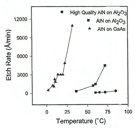
Fig1
We have observed a strong effect of annealing on subsequent wet etch rate of sputtered AlN films in KOH solutions, with over an order of magnitude decrease in rate after annealing at 1100o C.(36) Similarly the etch rate for In0.2Al0.8N grown on Si was approximately three times higher in KOH based solutions than for material grown on GaAs, which is consistent with the superior crystalline quality of the latter. Etching of InxAl1-xN was also examined as a function of In composition, with etch rate initially increasing up to 36% In and then decreasing to zero for InN.(36)
Minsky, White and Hu(37) reported laser enhanced, room temperature wet etching of GaN using dilute HCl/H2O or 45% KOH/H2O, with rates up to a few thousand angstrom/min for HCl and a few thousand angstrom/min for KOH. The mechanism is believed to be photoenhancement of oxidation and reduction reactions in what amounts to an electrochemical cell. Etch rates were linearly dependent on incident HeCd laser power.
上一篇: 氮化镓的大面积光电化学蚀刻