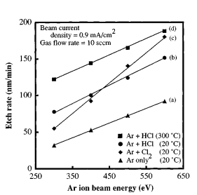
Recent progress in the dry etching of high quality III-V semiconductor nitrides, in particular GaN,1–8 has overcome one obstacle toward the realization of novel optoelectronic devices with blue to ultraviolet ~ UV! spectrum capabilities. Dry etching techniques are necessary to obtain vertical and smooth sidewall profifiles for optoelectronic device applications especially for laser facets and mirrors. Chemically assisted ion beam etching ~ CAIBE! 9 has become an important technique for facet and mirror fabrication in both AlGaAs/GaAs10 and InGaAs/AlGaAs11 material systems. In the CAIBE process, the sample is simultaneously exposed to a reactive gas and an inert gas ion beam. This confifiguration allows for the physical ~ ion beam energy and current density! and chemical ~ gas flflow! etching components to be independently controlled. The substrate temperature also plays a critical role in the chemical etching component and must be carefully controlled to obtain reproducible etch rates and anisotropy as has been demonstrated for InP12 and GaNbased1,3 materials. By optimizing the ratio of chemical assistance to ion flflux, vertical sidewall profifiles have been obtained in GaAs-based13 and InP-based12 materials. In our previous work with CAIBE of GaN in using an Ar ion beam and Cl2 gas, near-vertical etched sidewall profifiles were obtainable under all the etching conditions investigated.1,3 These conditions consisted of a wide range of chemical/ion flflux ratios and included the utilization of elevated temperatures of up to 300 °C. The best profifiles had sidewall angles of ; 4° to 5° from surface normal on structures etched 1 m m deep1 and ; 6° to 7° on structures 1.7 m m deep.3 These results, however, are not adequate for the realization of facets and mirrors in GaN and related materials. To improve anisotropy, a higher chemical component is required since overcut profifiles typically indicate a strong physical mechanism in the etching process. This observation led to the decision of using HCl gas since the H may add a method of chemically removing N as volatile NHx products.
The CAIBE process for this work was performed in a modifified Varian/Extrion RE-580 ion beam etching system. Details of this system have been discussed previously.1,3 The GaN used in this work was grown epitaxially on sapphire ~ 0001! substrates using metal-organic chemical vapor deposition ~ MOCVD! . The samples were unintentionally doped with carrier concentrations of ; 23 1017 cm2 3. The thickness of the epitaxial GaN layers varied from 4 to 5 m m. Samples used to determine etch rates used SiO2 as the mask. Etch depths were measured using a Tencor profifilometer after mask removal in dilute HF. The samples used for etch profifile studies were patterned with a SiO2/Ni mask structure using metal liftoff techniques and reactive ion etching ~ RIE! with a CHF3 plasma. Plasma-enhanced chemical vapor deposition ~ PECVD! and electron beam evaporation were used to deposit the SiO2 and Ni, respectively. After mask removal in dilute HF, profifiles were then examined using a scanning electron microscope ~ SEM! . AES analyses of unetched and etched GaN surfaces were performed in a Physical Electronics Scanning Auger Multiprobe 660 system using a 5 kV electron beam.
Figure 2 shows an Arrhenius plot of etch rate as a function of 1000/T. Etching was conducted at a current density of 0.6 mA/cm2 and a HCl gas flflow of 10 sccm. Curves ~ a! and ~ b! show etch rates using beam energies of 300 and 500 eV, respectively. Etch rates increase approximately linearly with substrate temperature at 300 eV. However, etch rates at 500 eV exhibit a nonlinear trend in which only temperatures above 200 °C provide chemical enhancement of etch rate. The increase in etch rates above 200 °C may indicate that the substrate temperature as well as beam energy plays an important role in the formation of Cl radicals. Preliminary work with InP using HCl gas has demonstrated a similar temperature dependence, suggesting that this increase in etch rate is not characteristic of the particular chemical reaction with the substrate material but is instead related to the supply of reactants.

Fig1
Auger electron spectroscopy was used to investigate surface stoichiometric changes resulting from the processing. Samples were etched for 5 min using conditions of 500 eV, 0.6 mA/cm2, and 10 sccm of HCl flflow. Samples etched at 20 and 200 °C both showed increased O intensity peaks and a reduction in N peaks on the surfaces in comparison to the unetched sample. The increased O may be the result of N defificiencies created on the surfaces by the etching process which subsequently allows for GaOx formation upon atmospheric contact. Oxygen atomic concentrations of ; 4%, 27%, and 11% were found on the surfaces of samples that were unetched, etched at 20 °C, and etched at 200 °C, respectively. Atomic concentrations of N on the respective surfaces were ; 31%, 6%, and 24%. Chlorine residue was found on the surfaces of the as-etched samples of ; 2–3 at. %. The stoichiometry of etched surfaces, however, could be restored to nearly their original unetched state by using a HCl:H2O ~ 1:2! dip.
The authors gratefully acknowledge Dr. R. Powell of Varian Associates for equipment donation and the technical assistance of N. Finnegan for AES analysis. Discussions with C. Youtsey on the CAIBE process are also acknowledged. The material work at APA Optics was supported by Air Force Offifice of Scientifific Research under Contract No. F46920-93- C-0059 and the work at the University of Illinois was supported by NSF Grant 92-02294.
上一篇: GaN、ZnO和SiC的湿法化学蚀刻
下一篇: GaN清洗程序分析