1. Introduction
A number of groups have investigated GaN cleaning procedures for device fabrication [1–5]. The importance of properly cleaned surfaces for ohmic and Schottky contacts deposition is well known [4,5]. There is currently no standard method of preparing the GaN substrate prior to metallization. Preparation methods differ from one laboratory to the other. Wet and dry etching methods are widely used in surface preparation for removal of surface contaminants. In addition, the morphology of the surface of the substrate prior to metallization has an inflfluence on the continuity of the ultra-thin metals used in fabrication of Schottky barrier diodes for UV detection. Wet and dry cleaning of substrates using chemicals have been used on GaN prior to metallization. Dry cleaning methods are known for introducing damage to the surface, usually making the material electrically unsuitable [6]. Various surface analytical techniques such as Auger electron spectroscopy (AES), X-ray photoelectron spectroscopy (XPS), low energy electron diffraction (LEED), and secondary ion mass spectroscopy (SIMS) have been used to identify the surface contaminants, oxides, metal particulate and reconstruction. Atomic force microscopy (AFM) has been used to monitor the surface cleanliness as a function of topography [7,8].
The use of HCl, NH4OH and HF solutions were found to remove the oxides effectively. A 1:1 HCl:DI solution was found to produce the lowest C/N ratio with a disadvantage of Cl addition to the surface. The O coverage on the HCl sample was found to be inversely proportional to Cl detected on the surface. According to their results, the fact that the N–Cl bond strength is less than that of Ga–Cl gave an explanation why there is Cl residue on GaN surface. The results of using H2SO4 and H3PO4 were observed residues of SO4 and PO4 on the surfaces of GaN, increasing surface oxide coverage after these treatments. The 1:10 HF-based cleaning solutions were found to increase the O/N ratio with no detection of F on the surface. Stoichiometric GaN surface was produced after annealing the surfaces at 700–800 8C in NH3. Using thermal desorption, it was found that HCl cleaned samples showed complete desorption of all contaminant species on the surface after 950 8C. AFM was used to investigate the surface roughness of the cleaned surfaces. All samples had surface RMS roughness comparable with the as-grown material, while H3PO4 resulted in increased surface roughness from as low as 20 A˚ to as high as 200 A˚ . On the GaN surface, the RCA SC1 and SC2 reduced the UV/O3 oxides, though SC2 left more C on the surface relative to SC1.
2. Experimental
n-GaN samples of orientation (1 0 0 0) and unintentional doping of 1.6 1016 cm 3 were obtained from AIXTRON, grown by metal organic chemical vapor deposition (MOCVD) on sapphire (Al2O3) substrate. The thickness of the GaN layer was 1 mm. The cleaning methods used are summarized in Table 1. All samples were fifinally blown dry with compressed nitrogen gas of ultra-high pure quality. Only analytical grade quality chemicals were used and all water rinses were done in deionised water (r > 18 MV cm). All samples used in this study were cut from the same wafer as GaN growth techniques are not yet well established as compared to other semiconductors. Ultrasonic rinse was employed to ensure the removal of all loose debris on the surface. All cleaning equipments used were made of pure quarts glass and Teflflon. Samples were loaded into the AES immediately after wet chemical cleaning.

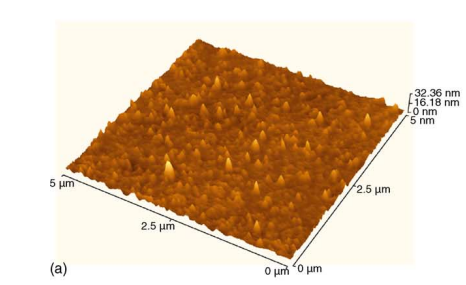
Fig1
There had been reports of improved electrical characteristics of metals/GaN contacts after treatments in HF, HCl, and NaOH. Miller et al. has reported the reduction of reverse bias leakage current in GaN Schottky diodes after treatment in NaOH. The high concentration of OH-ion on the GaN surface is attributed to the reduction of reverse bias leakage in their Schottky contacts [14]. In another report, Lin and Lee has reported the reduction of surface states on InGaN using (NH4)2S [15]. Electrically, (NH4)2S was reported to reduce the Schottky barrier height. In particular, it was reported that Ga–O, In–O and C–O bonds were removed from the InGaN surface after (NH4)2S treatment. Furthermore, repeated exposure of the surface that has a Cl peak to the electron beam in the AES system has resulted in desorption of the surface contaminants, and consequently, complete removal of the Cl peak.
To further analyse the cleaned surfaces, the ratio of Ga/N, and RMS surface roughness are plotted as a function of cleaning method, as shown in Fig. 5. There is a relationship between the RMS surface roughness and the contaminants on the surfaces, which conse quently affects the Ga/N ratio. The as-grown surface shows a very high surface roughness and Ga/N ratio and the cleanest surface shows lowest surface roughness and Ga/N ratio. Therefore as the surface is cleaned, the surface roughness reduces as the Ga/N ratio improves, implying that the chemicals used has etch GaN surface to remove contaminants. The RMS surface roughness of KOH etched surface, differ from the as-grown surface by about 0.4 nm. Different wet chemicals used previously in removing contaminants on GaN have shown no effect on the surface roughness of the material [2,3]. The work done previously to etch and remove surface GaN to form etch steps were not achieved by using HCl and KOH [16]. Ultraviolet light illumination and addition of ions were used to etch GaN successfully in KOH [17].
下一篇: 硫酸-过氧化氢-水系统中砷化镓的化学蚀刻