1. Introduction
Tiny bubbles are a promising candidate for anenvironmentally friendly method of photoresistremoval. It has been demonstrated that ozonemicrobubbles remove photoresist on a siliconwafer, even after the photoresist have beendamaged by a high-dose ion-implantation (1]. Butsignificant challenges are still remained, partlybecause the removing rate is not enough first forthe usage of microbubbles in the semiconductormanufacturing industry. Therefore, we need toenhance the removing ability of microbubblesthrough the clear understanding of the functionalmechanisms of microbubbles for the removal ofphotoresist layers. The purpose of the present studyis to clarify the effect of microbubble on thesurface of photoresist layers.
2.Characteristic of microbubbles relating tophotoresist removal
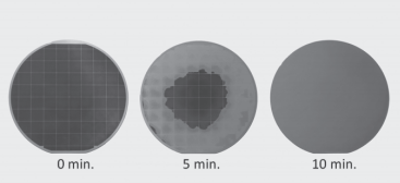
Microbubbles are tiny bubbles in aqueoussolutions and their diameter may be less than 50micrometer. The bubbles gradually decrease in sizedue to the dissolution of interior gases to thesurrounding water and eventually disappear underwater. This character enables the tiny bubbles toacquire promising functions, such as the increaseof interior gas pressure and the accumulation ofsurface electricity during the collapsing process oftiny bubbles (2-6]. Figure 1 shows photographs of a high-dose ion-implanted photoresist wafer beforeduring and after the ozone microbubble treatmentThe wafer was treated through a single wafer spincleaning method, and the ozone microbubble waterwas poured on the center of the wafer held on aspin table. Considering the treatment condition itmight have been reasonable to anticipate that thecleaning process would start at the center of waferand extend to outer part, such as the case of a merebaked photoresist shown in Fig. 2. But the resultindicated the contradict pattern for the high-doseion-implanted photoresist, and the layer ofphotoresist was stripped, instead of dissolution.from the outer edge to the center of the wafer.These results enable us to obtain an importantinformation considering the practicalusage ofmicrobubble in photoresist removals.
3. Experimental procedure
Figure 3 shows a schematic of the microbubblegeneration system used in the present study, and allparts of the system in contact with water are madeof metal-free Teflonmaterials.It wasadepressurizing type of microbubble generator(SHIGEN-KAIHATU CO.,INC.). A diaphragmpump introduced both of water and gas through itsintake line, and discharged them through adissolution tank in which the gas was effectivelydissolved in water under a pressure ofapproximately 0.4 MPa. The water containing thedissolved gas was then released by a dispersingnozzle. Turbulent flow in the nozzle caused thegeneration of microbubbles through bubblenucleation under a supersaturated conditionproduced by the rapid pressure reduction to theambient. Figure 4 shows the bubble sizedistribution of generated oxygen microbubbles insuper-purified water at around 20°C in a cleanroom. And it was observed that the sizedistribution changed according to the temperatureof water.

Fig1
As the samples for the present experimentalstudy, high-dose ion-implanted photoresists wereused as one ofthe most challengeable targets in thesemiconductor manufacturing [7, 8]. Siliconwafers spin-coated with a high-resolution positivephotoresistfor KrFlasertypeexcimer(TDUR-P3116EM 15CP, TOKYO OHKA KOGYACO., LTD.) and patterned by an exposure toolWafers were implanted with arsenic ion at doses of1E15/cm2 and an energy of 55keV, and were alsoimplanted with boron ion at doses of 1E15/cm2and an energy of 1lkeV The wafers were dicedinto samples with a size of 20*20mm2, and a dicedsample was placed on a spin table by a stick tapein-between the center and the edge of the table.
Inner part of the layers, a part of the bulk resistwas removed, and the top and the side walls ofcrust layers were remained. Hot water withoutoxygen microbubble was also evaluated by thesame method at the temperature of around 70 °Cand we could not observe such a significantdamage on the photoresist layers.
上一篇: 混合铝蚀刻剂的化学特性
下一篇: 用于 CVD金刚石沉积的氮化硅表面预处理