I. Introduction
SILICON NITRIDE (Si3N4) based ceramics are considered adequate substrates for growth of chemical vapor deposition (CVD) of diamond films for mechanical applications1–19 since they are hard and tough and, above all, they exhibit a thermal expansion coefficient close to that of diamond. This minimizes the interfacial residual stresses between the film and the substrate and ensures superior adhesion.20 Additional advantages of Si3N4 are its carburizing nature and the absence of phases that catalyze the formation of graphite, as happens with the cobalt binder in the case of hard metal substrates.9
The aim of the present work is to systematically study the effect of conventional Si3N4 chemical etching procedures and microflawing techniques for CVD diamond deposition on this tool material. Nucleation densities, homogeneity, and diamond film crystal sizes are compared. A self-consistent approach is made using blank samples whose “inert” surfaces are guaranteed by polishing all samples with colloidal silica, avoiding the presence of diamond particles before pretreatment procedures.
II. Experimental Procedure
Dense disk-shaped Si3N4 substrates ( 15 mm) for diamond deposition were pressureless sintered at 1750°C for 2 h under N2 atmosphere, inside powder-bed Si3N4/BN protected graphite crucibles. The chosen sintering aid composition was selected after a study of the intergranular glassy phase role on the CVD diamond nucleation.3 Batches with -Si3N4 (Grade M11, H. C. Starck GmbH and Co., Germany), Y2O3 (Grade C, H. C. Starck GmbH and Co., Germany), and Al2O3 (Alcoa A-16SG, Alcoa Industrial Chemicals, Bauxite, AK) in weight proportions of 89.3%, 7.0%, and 3.7%, respectively, were then used.
III. Results and Discussion
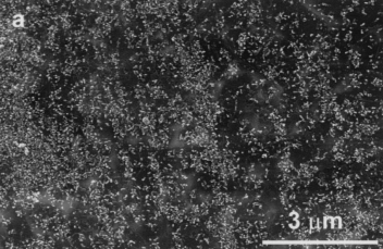
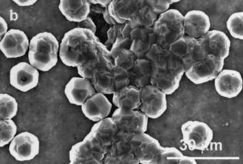
Figures 1(a) and (b) are representative SEM micrographs of the Si3N4 as-polished (NT) surfaces, respectively, after 10 min of diamond nucleation and 6 h of diamond growth. A low density of nuclei appears randomly distributed on the Si3N4 substrate without evidence of preferential sites concerning the substrate phase distribution. The initial H2 etching period before methane introduction in the reactor was insufficient to allow a preferred attack of the intergranular glassy phase, contrary to other reports.14 The bright appearance of the diamond nuclei is due to the charge effect. After 6 h of diamond deposition (Fig. 1(b)) agglomerates of 10 m average sized, well-shaped diamond crystals, were obtained instead of a complete film.


Fig1
III. Results and Discussion
Figures 1(a) and (b) are representative SEM micrographs of the Si3N4 as-polished (NT) surfaces, respectively, after 10 min of diamond nucleation and 6 h of diamond growth. A low density of nuclei appears randomly distributed on the Si3N4 substrate without evidence of preferential sites concerning the substrate phase distribution. The initial H2 etching period before methane introduction in the reactor was insufficient to allow a preferred attack of the intergranular glassy phase, contrary to other reports.14 The bright appearance of the diamond nuclei is due to the charge effect. After 6 h of diamond deposition (Fig. 1(b)) agglomerates of 10 m average sized, well-shaped diamond crystals, were obtained instead of a complete film.
According to a previous study,3 the chemical nature of the amorphous intergranular phase of the Si3N4 materials was found to be deleterious for diamond nucleation. This is a controversial matter, as the opposite view has been advanced by other authors,14 in contrast to others.11 The results after the CF4 plasma attack, which preserves the glassy phase, corroborate this model, as almost no diamond nuclei are detectable at the CF sample surface (Fig. 2(c)). The absence of diamond crystallites on the Si3N4 grains comes after the strong chemical modification of the crystal surfaces by Si fluorination, as explained before. This type of Si3N4 etching procedure is exactly the opposite of the acid and basic attacks that selectively remove the glassy phase and expose the remaining reactive area to the H2 plasma.
上一篇: 微气泡对光刻胶层的影响
下一篇: 多晶金刚石薄膜技术