I. INTRODUCTION
The presence of sp3 C–C bonds in the diamond lattice leads to its unique mechanical, chemical, optical and thermal properties not matched by any other known materials. Consequently, diamond becomes a unique material for a number of applications including microsystems and microelectromechanical systems s MEMSd , especially at high temperatures and in harsh environments. The diffificulty to fabricate the sp3 C–C bonds, which delayed the production of chemical vapor deposition s CVDd diamond until 1952–53, is now causing a delay in the development of a reliable diamond microfabrication technology that is compatible with conventional microsystems/MEMS technologies. Since there is no reliable large-area diamond hetro-epitaxial technology available today, a number of studies have focused on inexpensive polycrystalline diamond s poly-Cd growth mainly over small size Si wafers s less than 2 in.d . Although some studies used 4 in. Si wafers as substrates,1,2 most of the reported work has focused on small size substrates to demonstrate poly-C fifilms for temperature sensors and heaters,3,4 piezoresistive sensors,1,5 gas/chemical sensors,6,7 radiation sensors8,9 fifield emission and optoelectronics devices,10–12 MEMS packaging,13 and RFMEMS resonators.14,15 Most of these studies, although primarily motivated by industrial applications, were limited to laboratory scale devices with less emphasis on scaling, cost and reproducibility.
II. POLY-C MICROSYSTEMS TECHNOLOGY
The poly-C microsystems technology development focuses on high-density diamond seeding, large area fifilm growth, boron doping of poly-C, patterning through dry etching, Ohmic contacts and process integration. P-type 4 in. Si wafers with a 2 m m thick SiO2 layer were mainly used as a substrate material in this study. The diamond growth conditions are shown in Table I.
A. Seeding
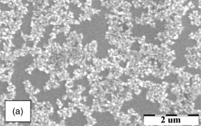
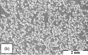
The CVD growth of poly-C fifilms requires a pretreatment step to generate seeds s or nucleid on the substrate before the growth begins. Surface abrasion,16–18 ultrasonic in diamond powder loaded solution,19 bias enhanced nucleation s BENd , 20–22 spinning of diamond-powder-loaded photoresist s DPRd , 23 and spraying of diamond-loaded flfluids24,25 are typically used for the pretreatment as shown in Table II.
B. Growth
Poly-C can be grown using a variety of CVD methods including microwave plasma CVD s MPCVDd , 28,29 hot fifilament CVD,30,31 radio frequency s RFd CVD and dc-arc jet CVD s Ref. 32d as seen in Table IV. However, MPCVD is the most widely used technique for electronic and optical applications because of its effificacy to produce high fifilm quality, large substrate size, less contamination and better controllability.
For the results reported in this work, a bell jar type MPCVD chamber s Wavemat™ MPDR 313EHPd was used with a 9 in. chamber diameter and 5 in. quartz bell jar diameter. A 2.45 GHz, 5 kW microwave power supply s Sairem™, GMP60KSMd and a large chamber size ensured the uniformity of the plasma and the poly-C growth on 4 in. size substrates. The sample wafer was heated by the plasma and its temperature was monitored by a pyrometer. The detailed growth conditions are listed in the Table I. Trimethylboron s Bs OCH3d 3, TMBd diluted in hydrogen s TMB/H2=0.1% in volume ratiod was introduced during the poly-C growth environment for the in situ boron doping.


Fig1
III. CONCLUSIONS
An IC compatible poly-C thin fifilms fabrication process was realized on a 4 in. oxidized Si wafer using the DPLW spin, high power MPCVD, and ECR-assisted reactive ion etching technologies. The new DPLW spin method can give a uniform seeding density of 23 1010 /cm2 over the 4 in. wafer. The optimized growth exhibited a power effificient large area growth with less than 25% thickness variation over the 4 in. wafer. ECR-assisted reactive ion etching with microwave plasma was carried out using SF6 /O2 /Ar gases with an etch rate of 80 nm/min and less than 7% variation over the 4 in. area.
上一篇: 用于 CVD金刚石沉积的氮化硅表面预处理
下一篇: 硅的湿化学蚀刻机理