1. Introduction
ZnO has been of great interest recently because of its wide band gap (3.36 eV) and relatively large exciton binding energy (60 meV) at room temperature (RT), which make this material a promising candidate for light emitting devices and semiconductor lasers with low thresholds in the ultraviolet (UV) region [1,2]. Compared with GaN, ZnO possesses many unique properties mainly including the availability of high quality ZnO substrate and the simpler wet etching processing at safe temperature, these advantages are especially attractive for some device applications such as solar cells [3], photo detectors [4], acoustic devices [5], gases sensors, etc. [6]. Despite the diffificulty in p-type doping, some ZnO based light emitting diodes (LEDs) have been reported recently [7–10]. For the fabrication of devices such as LED and laser diode (LD), mesa formation through controllable and uniform etching process is indispensable if nonconductive substrates were used. As yet,most ofthe ZnO etch processing were dominated by dry etchingbecause of its controllable etching rate [11-13]. Compared withthe dry etch, the wet etch technique possesses the advantages ofsimplicity and low equipment cost. ZnO is easily etched in allacids and alkalis [14]. Nevertheless, the etching rate for ZnO inmost single acids, mixed acids and alkalis is very fast, even ifthe solution concentration drastically reduced f15]. There hasbeen no report on the systematic investigation of the influenceof wet etching on morphology, optical and electrical propertiesof ZnO films.
2. Experimental procedures
ZnO thin fifilms were deposited on c-plane Al2O3 substrates by ablating a ceramic ZnO target (99.99%) using a KrF excimer laser (248 nm, 5 Hz). The substrate surface was sequentially degreased in ultrasonic baths of methylbenzene, acetone and ethanol, then etched by a mixture of H2SO4:H3PO4 (3:1) at 160 8C for 15 min. During fifilm deposition, the laser energy density was kept at 2.5 J/cm2 . The distance between the substrate and target was 5 cm. The substrate holder was rotated at a rate of 20 rpm to obtain uniform fifilms. ZnO fifilms were grown at 650 8C for 200 min under 60 Pa in oxygen ambient. The thickness of all the samples was about 500 nm.
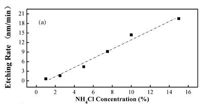
NH4Cl aqueous solutions of different concentrations were prepared by dissolving high-purity (99.99%) NH4Cl powder in deionized water (r > 18 MV cm). For investigation of the dependence of etching rate on the concentration, ZnO fifilms were etched in NH4Cl aqueous solutions with different concentrations in the range of 1–15 wt%. In order to study the relationship between etching thickness and etching time, ZnO fifilms were etched by a selected concentration of 5% NH4Cl solution for different time and then washed by deionized water immediately.
It can be concluded that the linear relationship between etching rate and NH4Cl concentration is attributed to the linear increasing of the H3O+ number with thickening of the NH4Cl aqueous solution. Fig. 2(b) shows the dependence of depth on etching time for the fifilm etched in 5% NH4Cl aqueous solution. The good linear dependence indicated that the etching depth is controllable in our process.
The PIL measurement was performed to investigate the effectof etching treatment on the optical properties ofZnO thin film,as shown in Fig. 4. As can be seen in the spectra, all the PIspectra show two peaks. For the as-deposited film, the nearband edge (NBE) emission around 380 nm is relatively strongand is accompanied by a rather weak deep level (DL) emissionband at around 500 nm. The NBE emission is generallyascribed to the exciton emission (20], and the DL emission isattributed to oxygen vacancies [21] or zinc interstitials (22]. PLmeasurement suggested that the as-grown films are of opticalhigh quality with minor defects. It was found that the intensityof NBE emission becomes weaker and the intensity of the Dlemission becomes stronger with increasing of the etching time.

Fig2(b)
The electrical parameters ofZnO films were investigated byHall effect measurement. Moreover, reproducibility investiga-tions have also been performed for three samples. The numberof measurements, average alue and standard deviation arelisted in Table 3. As the etching time increased, the resistivity(R) increased slightly, at the same time the Hall mobility (p)decreased. After being etched for 30 min, the mobilitydecreased from 9.37 to 5.04 cm2 y-' s-1and the carrierconcentration (n) did not change obviously within this range.We also found that the S.D. is comparatively small. Theelectrical parameters were the statistical measuring results fromthe whole film (including the surface and under layer). Thethickness of the film decreased with the increasing of etchingtime and the surface scattering contributing to the mobilitybecame noticeable accordingly. After etching, ZnO films got rougher and the defects resulting from the etching treatment increased. All these factors strengthened the surface scattering, as a result the Hall mobility reduced and the resistivity increased accordingly. The exact origin and mechanism for the obtained electrical parameters have to be verifified by further research.