Recent progress in the wide bandgap III–V nitrides has revealed this material system of outstanding thermal, electronic, and optical properties compared with those of group IV and II–VI materials.1 A plethora of research activity has been emphasized on the device work such as for short wavelength emission,2 detection,3 and high temperature electronics applications.4 This has brought in the success of high brightness blue/green light emitting diodes in the market,5 and more recently the continuous wave room temperature laser diodes.2 Although much attention has been focused on device applications, little has been devoted to the issues of wet etching upon which the chemical stability of III–V nitrides continues to challenge the technology development. Common practice has therefore pursued the dry etching techniques to resolve the problems. Among which a suitable choice of flfluorine, chlorine, iodine, or methane-based chemistries is important in minimizing the surface damage caused by the high-density plasma.6 It is therefore desirable to have alternative nitride etching methods which are immune to such effects.
To date there has been little success in the development of wet etching techniques for III–V nitrides. Aluminum nitride ~ AlN! 7 and indium nitride ~ InN! 8 are the only known epi-materials that can be etched in hot alkaline solutions. Gallium nitride ~ GaN! , on the other hand, appears to be more resistant upon such a treatment. It has been noted that thermal treatment up to 85 °C on common acids can hardly etch GaN.9 Conventional wisdom has ascribed the cause of such diffificulties to a lack of suitable oxidation and reduction processes in the etchants.
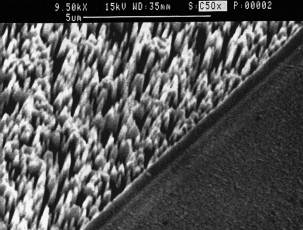
Figure 1 shows the SEM micrograph of a one-hour PEC treated GaN in a H3PO4 electrolyte of pH5 3. Growth of needle-like crystallites is clearly seen along the GaN growth direction. These microcrystallites are transparent in the visible and can be dissolved separately in a 2 M KOH solution. In Fig. 2 we compare the energy-dispersive x-ray analysis ~ EDX! data of these microcrystallites with those of as-grown GaN samples. The dramatic increase of oxygen counts in the former clearly indicates a rich oxide content in these microcrystallites. In contrast to previously reported thermal-grown oxides showing multiple diffraction peaks on GaN,20 these microcrystallites reveal only one single peak at 2u 5 34.46° from an x-ray diffraction ~ XRD! measurement using a Cu Ka radiation. From a comparison with the established diffraction patterns of gallium oxide (Ga2O3),21 we identify these microcrystallites as b -Ga2O3 . To our knowledge, this is the fifirst time the PEC technique has been successfully applied to grow microcrystallites of Ga2O3 on GaN.

Fig1
An important reason for studying the oxidation process is that the dissolution of III–V semiconductor always involves a change of the oxidation state.10 For example, in a wet oxidation process, charge transfer takes place at the semiconductor/electrolyte interface.22 A calculation made by Boudreaux et al. on double layer tunneling at the semiconductor/electrolyte interface has indicated the process of hot carrier injection can energetically initiate such reactions at the interface.23 We thereby attribute the growth of microcrystallites Ga2O3 to the deep-UV-enhanced oxidation of GaN upon which the UV-excited hot carrier injection at the GaN/electrolyte interface assists the process.
The evidences showing UV-enhanced oxidation of GaN in Figs. 1 and 2, moreover, signify a decisive oxidative dissolution process that is suitable for making a PEC etching of GaN. Shown in Fig. 3 are the pH dependent etch rates of GaN in aqueous KOH and H3PO4 solutions, respectively. We fifirst note an amphoteric solubility of GaN in the pH regime from 2 1 to 2 and 11 to 15. We also observe a peak etch rate of 125 and 90 nm/min in the H3PO4 and KOH solution at pH5 0.75 and 14.25, respectively.
上一篇: 铝蚀刻剂研究
下一篇: 盐酸等溶液中GaAs和InP的选择性湿蚀