1. Introduction
Defect control is the most critical parameter in semiconductor manufacturing for yield enhancement and device reliability [1-4]. And as scaling down to sub-14 nm, the device failure ratio by small particle is increased accordingly [1]. In the semiconductor process, chemical mechanical polishing (CMP) is known as the dirtest process to contaminate wafer surface and it is difficult to control post CMP defect. However, device feature size shrinkage and device complexity require more CMP steps in the manufacturing and post CMP defect control becomes more complicated. CMP process uses slurry chemical to make material surface soften and abrarisve particle in slurry removes soften layer mechanically, which lead to global and local planarization of wafer [5]. And slurry chemical contains various polymeric additives for selectivity control and high material removal rate [5].
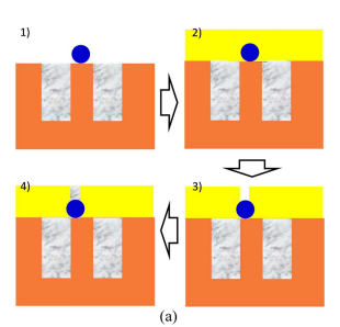
Hence, a lot of particles, organic materials and wear debris are generated during CMP process, such as abrasive particle, abraded wafer material, polishing pad debris, and particles from the polisher itself [6-7]. And most of defects from CMP process are potentially considered as yield-killing [1]. Examples of known device failure mechanism by non-metallic particle are shown in Fig. 1. Fig. 1 shows vertical structure of metal gate and contact patterning sequence schematically. Residual slurry abrasive particle defect from metal gate CMP can influence on post contact patterning directly as shown in Fig. 1(a). And organic residue itself may not kill the device directly, however post process interact with organics and causes leakage failure as given in Fig. 1(b). Organic residue at post metal gate CMP process can be removed by contact etch process and it can be filled with metal contact material, which causes leakage failure between layers as shown in Fig. 1(b). Historically, post CMP process has standalone ex-situ wet cleaning steps to remove CMP defects. However, device complexity and limitation of post CMP clean chemical make CMP process itself to remove CMPinduced defects as much as possible. In order to minimize post process defect, most CMP equipments have in-situ cleaning module in addition to polisher module. Depending on equipment maker, post CMP in-situ cleaning module is composed of megasonic cleaning, brush scrubber cleaning, high pressure fluid cleaning and their combination.

Fig1(a)
2. Experiment
Reflection-LK polisher from Applied Materials Inc. is used for the experiment. Schematic of the equipment is shown in Fig. 2(a). It is composed of 3 platens polishing module and in-situ cleaning module. And insitu cleaning module is composed of megasonic tank, 2 brush scrubber boxes (brush box 1 (BB1) and brush box 2 (BB2)), and isopropyl alcohol (IPA) dryer. For this experiment, megasonic tank is not turned on because the purpose of this paper is to investigate brush cross contamination effect only. For the brush treatment effect on defectivity, new brush is implemented with and without brush treatment, and experiment wafers are run periodically. However, in order to investigate effect of brush gap and brush contact sequence on the defectivity, brush is used over 500 wafers polishing processed before experiment wafers run. The picture of brush module is given in Fig. 2(b). Wafer is located in the middle of two brushes vertically. And both wafer and brushes rotate each other to remove wafer defects. Spray bars are installed above the brushes and chemical flows through spary bar. Deionized water (DIW) flows through brush core to soak brushes. 300 mm tetraethyl orthosilicate (TEOS) blanket wafers are used for the experiment. The thickness of TEOS is 3k Å for all experimental conditions. And all TEOS wafers are processed cleaning module only without polishing process. Acidic based cleaning chemical is used for both brush scrubber boxes with 2000 ml/min flow rate at main cleaning step for all experiments. Brush and wafer rotation speed are 400 rpm and 50 rpm respectively. From the experiment, effect of brush soaking treatment, brush break-in, and brush contact sequence on the post defectivity are explored. After processing of brush cleaning, surface defects are inspected by SP3 tool from KLA-Tencor and defect types are classified by scanning electron microscopy (SEM) review. The SP3 inspection bin size is 60 nm.
Experimental results in this paper address optimization of post CMP in-situ brush cleaning for advanced node semiconductor manufacturing. New brush is unstable at cross contamination aspect and it needs to be properly broken-in before actual wafer processing. And brush cleaning recipe optimization can reduce cross contamination and maximize particle removal efficiency. Although this paper is focused on the brush cross contamination and brush stabilization, the results introduced in this paper can give insights on post CMP in-situ cleaning optimization.
上一篇: 使用IPA溶液去除晶圆上静电荷
下一篇: 晶体硅光伏组件的腐蚀及其对性能的影响