1. Introduction
The experiments have demonstrated that, for the same sample, it is possible to obtain different pyramidal profifiles due to microloading effects and additive inflfluence. A wide array of applications is expected for this type of technology in the fifields of solar cell industry and MEMS microfabrication. This work was performed to study the etching profifile and angles of pyramidal structures to be used in biological cell penetration. Surface topography plays a crucial role, as these structures must be further processed through microfabrication methods.
2. Experimental Details
Experiments were carried out on 0.01–0.03 Ωcm, n-doped, 500 ˘ 25 µm-thick polished silicon wafers with a monocrystalline (100) orientation (Sil’tronix, Silicon Technologies, Archamps, France). After surface cleaning, with Alconox (Sigma Aldrich 242985 Alconoxr detergent, St. Louis, MO, USA) and IPA, a 300 nm thick Chromium layer was deposited by Magnetron Sputtering (Alcatel SCM 450: 3.07 mTorr, 20 sccm Argon, 20 WDC, 51 min [16]). Using Direct Writing Laser photolithography (Lasarray DWL2.0: positive resist PFR 7790 G 1.5 µm-thick [16]), square structures (8 to 40 µm) were defifined to study the effect of KOH wet etching and IPA inflfluence over the different crystallographic planes. Profifile alignment was performed using the wafers flflat and the DWL2.0 software, to a maximum deviation of 0.02 rad. The wafer was then diced in 9 mm ˆ 9 mm individual dies. The resist pattern was transferred to the Cr fifilm by wet etch (Sigma Aldrich 651826 Chromium Etchant, St. Louis, MO, USA). Finally, the Silicon surface is ready to be etched. Notice that any native oxide will be also etched during this process. Because silicon structures to be etched are less than 20 µm thick, the backside of the silicon wafer was left unprotected, with minor impact on the total wafer thickness. The schematic description of the process can be seen in Figure 2.
3. Results and Discussion
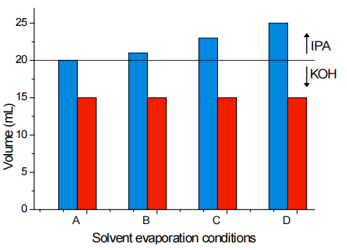
The IPA availability effect is reinforced by results of a parallel etching process, containing an initial volume of 20 mL dissolved KOH and 2 mL IPA, and then adding 2 mL IPA every 10 min, ensuring that IPA is always available during the entire etching process (evaporation rate of 0.175 mL/min was observed, as previously described). The macroscopic etching results from this experiment are quite similar from those obtained in Sample 4, and distinguishable from every other sample. The same etching profifile can be achieved either with an initial saturated solution, or with a lower, but continuously assured, concentration of IPA.

Fig2
Results demonstrate that IPA availability, and not concentration, plays an important role in the definition of the final structure. When working in an open system, where evaporation affects the chemical balance of the etching solution, we should take into account volumes rather than concentrations. IPA directly reduces the etch rate for the (110) plane, comparatively to the (100) plane. Therefore, longer availability of IPA during a reaction will originate structures with a wider base. However, for a long enough etch, the complete evaporation of IPA will allow the increase etch of the (110) plane, thus receding the base width, and (331) plane, converting square shaped to octagonal shaped structures. Nonetheless, if a steady supply of IPA is constantly added, to assure its availability, the same results are obtained as if a saturated concentration of IPA was always present.
An optimal volume of IPA is desired in order to obtain reproducible structures with the desired size and surface smoothness. In an open system, IPA can be added to the solution at any moment and its availability calculated from the evaporation rate. This fine tailoring of the etching conditions in a dynamic process may open up new possibilities for the precise control of the desired structures.
上一篇: 用于MEMS应用的玻璃湿法蚀刻
下一篇: 薄膜硅太阳能电池氧化锌的化学蚀刻