1. Introduction
Thin-film silicon solar cells rely on light trapping to improve their conversion efficiency from light to electrical energy. Often this is achieved by textured surfaces that scatter the light efficiently into the absorber layer. This texture has been introduced in the transparent front contact[1] or in reflectors.[2] Zinc oxide is one of such texturizable transparent contacts that can be prepared by sputter-deposition and subsequently textured by chemical etching on very large-area substrates.[3] Even though the chemical etching of crystalline ZnO has been investigated in the 1960s[4] and etching can be explained on the basis of a dangling bond model,[5] significant complexity arises from the polycrystalline nature of sputter-deposited ZnO thin films. Since the etch rate is strongly dependent on the crystalline orientation,[4, 6] anisotropic etching occurs on structurally heterogeneous ZnO films. Etching of ZnO has been utilized for light scattering in thin-film silicon solar cells[7] and therefore the need to understand the mechanism of structure formation upon etching of polycrystalline films has arisen. Several empirical studies investigated the influence of preparation and etching parameters to optimize the resulting light-scattering ZnO surface.[8] However, due to the complexity of the interrelation between preparation conditions, material properties, and etching process there is neither a microscopic understanding nor any empirical model available that sufficiently describes the resulting etched structures, based on information that are accessible prior to etching.
2.Empirical Growth and Etching Studies
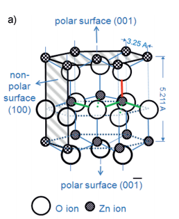
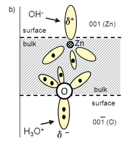
Both ZnO single crystals and polycrystalline films are readily etched in many acidic[4, 6, 9] and basic solutions.[4, 10] The etching behavior of the single crystal ZnO is well understood and can be explained by the wurtzite structure and a dangling bond model.[4–6, 11] Figure 1 shows the wurtzite structure (a) and a dangling bond model for etching at the polar surfaces (b). The surface atoms on the perfect polar faces are tightly bound to three adjacent atoms in the bulk material, while the atoms in the underlying layer are only bound to one atom in the bulk. These different bond structures between atoms inside the tightly bound double layers and from one of these double layers to the next are indicated by the green and red lines in Figure 1 a. Thus, the etch rate-determining step is to remove the tightly bound top atom. The partial positive and negative charges of the dangling bonds at the Zn(001) and O(00 1) terminated surfaces can easily be attacked by hydroxide (OH ) and hydronium (H3O+) ions. Due to the same charge type, the respective opposite attack is inhibited, such as H3O+ on the Zn-terminated surface. In this case, the attack of etching species can only occur at defects, such as screw dislocations, where the charge repulsion is disrupted. The model shows that the etch rates on the polar (00 1) face in acids is one order of magnitude larger than on (001) faces.[12] Note that such truncated crystal surfaces might reconstruct and relax in real crystals to minimize their surface energy.[13] However, most experimental findings on etching of ZnO are in agreement with the predictions of this model.


Fig1
3. Conclusions
This paper provides a literature review on wet etching of zinc oxide in acidic or basic solutions which serves as a background for the discussion of etching models. Recently, we performed some additional experiments to test previous assumptions or to clarify open questions regarding crater formation on polycrystalline films and single crystals of ZnO. Based on these experimental findings we proposed a three postulate etching model that allows us to qualitatively describe the etching behavior of ZnO thin films through the combination of physical and chemical aspects. Deposition conditions of the ZnO films determine the material properties that are modeled by mainly Zn-terminated grains, which are surrounded by grain boundaries of different etch potentials. These potentials depend on the degree of disorder between adjacent grains. The etching agent then defines a threshold by its effective size and mobility. If the etch potential of the grain boundary exceeds this threshold vertical etching along the grain boundary occurs and craters are formed. Lateral etching is related to the wurtzite structure of ZnO, and its relation to the vertical etch rate defines the shape of craters.
Experimental Section
ZnO single crystal wafers were purchased from Crystec, Berlin, Germany. The crystal wafers were cleaved from a hydrothermally grown ZnO crystal and polished on both (001) and (00 1) faces perpendicular to the c-axis. The (001) face was marked by a beveled edge. Doped (Al or Ga) or undoped ZnO films were prepared by sputter-deposition using different processes and deposition systems on various glass substrates. Most films were prepared in a vertical in-line sputtering system for 40 40 cm2 substrates, supplied by VAAT, Dresden, Germany.[10b] As an example, typical sputtering conditions are given for the “standard Jlich” ZnO:Al, that is sputtered from a planar 750 100 mm2 ceramic ZnO:Al2O3 (99:1 w/w%) target at a substrate temperature of 3008C and a pressure of 0.1 Pa pure argon onto a Corning Eagle XG 1.1 mm glass substrate. The plasma was excited by a radio frequency of 13.56 MHz and a power density of 2 W cm 2 . However, some ZnO:Al films were also reactively sputtered from metallic targets. More details on the specific processes are given in the references [8a, c, g, 9a, 10b, 21, 24, 25].
上一篇: 异丙醇酒精蒸发法对硅的动态湿蚀刻
下一篇: 碳化硅在碱性溶液中的阳极刻蚀