1. Introduction
There is strong renewed interest in silicon carbide (SiC) for device applications. With a favourable lattice constant and coeffificient of thermal expansion, it can serve as substrate for epitaxial growth of group III-nitrides [1]. In many application areas, for instance those related to aerospace, automotive and petroleum industries, there is a need for electronic devices that can operate at high power levels, high temperatures, high frequencies and in harsh environments. Silicon (Si) cannot meet these requirements; SiC can [2–4]. In addition, because of its exemplary chemical and mechanical properties SiC, in combination with Si, is fifinding wider application in sensors and micro-electromechanical systems (MEMS) [5–9].
2. Experimental details
Single-crystal 6H-SiC (n-type) and 4H-SiC wafers (n- and p-type) (0 0 0 1) were obtained from Cree (United States) and Umicore (Belgium). The n-type wafers were oriented on-axis, nitrogen-doped and had a resistivity varying between 0.01 and 0.07 cm. The p-type wafer (Cree) was oriented 8◦ off-axis, aluminium doped and had a resistivity of 3.86 cm. All samples used in this study had a Si polar face. For the electrochemical experiments, a circular opening was defifined on the samples using a Si3N4 mask. The diameter of the opening was 2 mm. Ohmic contacts to the p-type SiC were made by evaporating a 300 nm thick layer of Al/Ta/Au on the back side of the wafer. The metallized wafer was subsequently annealed at 850 ◦C for 10 min. The n-type wafers were contacted using a 300 nm Ti/Au layer followed bya1s annealing step at 1000 ◦C. The samples were mounted as a rotating disc electrode (RDE). Electrochemical measurements were performed in a three-electrode cell with a platinum counter electrode and a saturated calomel electrode (SCE) as a reference. For open circuit photoetching experiments, Ohmic contacts were made by evaporating a Ti layer, 100 nm thick, without any additional heat treatment.

Fig1
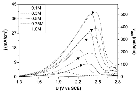
The inflfluence of temperature on the current–potential characteristics is shown in fifigure 2(a). The experiments were performed in 0.1M KOH solution. The peak current density depends strongly on temperature; it increases exponentially with increasing temperature. The etch rate, depicted on the right axis of fifigure 2(a), increases by a factor of 2.55 on a 15.3 ◦C temperature increase.
The analysis of the images obtained after this two-stage etching procedure allows us to understand the peculiar etch features formed during E+M etching of some SiC substrates (as shown in fifigure 6(a)). Apart from the typical dislocationrelated etch pits, numerous comet-like grooves were formed, which evidently represent segments of dislocations inclined with respect to the surface under small angles. Similarly, the ridges due to photoetching in fifigure 6(b) are formed on dislocations parallel to the surface and pinned by a cluster of macro-pipes.
上一篇: 薄膜硅太阳能电池氧化锌的化学蚀刻