1. Introduction
Most of the technological applications of silicon (Si) in semiconductor device manufacturing are based on the specifific interface properties of this material. Silicon dioxide (SiO2), which can be prepared on Si surfaces by simple oxidation methods, is characterised by high chemical and electrical stability. The dominance of crystalline silicon in photovoltaic applications- in nearly 90% of the worldwide solar cell production is based on multi- and mono-crystalline substrates, that can be ascribed partly to the knowledge about this material, which has been accumulated in recent years in microelectronics technology. Decisive preconditions to the development of economically attractive solar cells are the reduction of material consumption, the simplifification of technological processes and further improvements of the energy conversion effiffifficiency. As a result of rapid advances in silicon solar cell manufacturing, various solar cell concepts using thin fifilm-technologies for saving material have been developed. For the amorphous/crystalline silicon (a-Si:H/c-Si) hetero-junction, an inherent advantage, as compared to conventional diffffused p/n-junctions is the possibility to choose materials, layer thicknesses, and dopant concentrations for their construction which are best suited for a-Si:H(n, p)/c-Si (n, p) hetero-junction solar cells. In thin fifilm structures however, the interfaces take up a greater part of the solar cell concerned and interface defects, resulting in rechargeable interface states that become increasingly more critical. The development of effiffifficient light trapping structures and minimization of interface recombination losses become a key issue for further development of silicon solar cells technologies. Increasing attention has also therefore been focused on the in-situ monitoring and control of surface morphology and surface electronic properties during wet-chemical pre-cleaning treatments - carried out before preparation of thin oxides, a-Si:H/c-Si hetero-junctions, passivation layers and contacts [1, 2].
2.Wet-chemical substrate texturization and pre-treatment
Using n- and p- type Si(100) Wafer (2-5 Ω cm, doped by P and B, respectively), two types of substrates with (a) as cut and (b) polished surfaces were treated fifirst to remove saw-damage and / or to obtain the light trapping textures followed by wet-chemical oxidation and etching treatments to reduce the preparation-induced microscopic surface roughness in the mono-layer range. Difffferent surface textures were obtained (1) by anisotropic etching in an alkaline potassium hydroxide / isopropyl alcohol (KOH/IPA) solution at 80°C, (2) using an isotropic texture etch (TE) transferred from the wafer thinning technology [8].
3. Surface morphology and optical re- flflectance on isotropic and anisotropic etched substrates
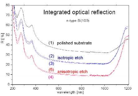
In solar cell manufacturing, wet-chemical etching procedures applying alkaline or acidic solutions are preferred to remove saw-damage - shown in (Fig. 1a) - from the ascut wafers in order to avoid expensive and time consuming lapping (Fig. 1b1) and polishing processes (Fig. 1b2). Additionally difffferent texturization schemes of silicon substrates are utilised in high effiffifficiency solar cells to enhance anti-reflflection properties through multiple bounce incidence of light at the front surface, the path length for absorption and internal reflflection at the back surface. Randomly distributed pyramids, prepared by an-isotropic etching in alkaline solutions (Fig. 1c), based on sodium- (NaOH) or potassium hydroxide (KOH), are utilised to optimise the light trapping properties in mono-crystalline Si(100) substrates [13]. Alkaline etching solution requires a substantial amount of energy to keep the etch baths at the required temperature. Another issue is the limited solubility of the reaction product potassium flfluorosilicate (K2SiF6), which can be a limiting factor in bath lifetime and throughput [8].

Fig1
The fabrication of effiffifficient silicon solar cells with minimized interface recombination losses, however, requires not only extremely clean and undamaged Si interfaces but also low densities of interface states. The relation between interface state densities and structural imperfections at silicon surfaces has been intensively investigated, because the reduction of their densities is a main problem in the microelectronic device technology [16].
According to our recently reported results, a strong correlation between preparation-induced surface microroughness on the nm scale and density of interface states was observed. The large number of crystallographic defects on edges and step on the rough interface are assumed to be the result of faster etching attacks on RCA cleaned substrates with Si(111) pyramids (curve 5), compared wet-chemically smoothed Si(111) pyramids (curve 6), and to polished Si(111) and Si(100) substrates (Fig. 4, curves 1…4).
上一篇: 碳化硅在碱性溶液中的阳极刻蚀