1. Introduction
Information technology (IT) has brought immense transition on our modern society. To enhance memory density of the IT devices, semiconductor is fabricated into extreme-scale integration without leakage current using the shallow trench isolation (STI) [1] technique. In this process, solid-phase silicon nitride (Si3N4) layer plays as a mask in partial silicon dioxide (SiO2) deposition. Through this deposition, a vertically stacked structure is formed consisting of hundreds of alternately stacked atomic layers of Si3N4 and SiO2. The Si3N4 mask has to be removed at the end of the procedure, typically by thermochemical etching. Therefore, selective and complete etching of Si3N4 over SiO2 is a key step in the STI technique to fabricate the high-performance semiconductor devices.
2. Computational method
All fifirst-principles calculations were performed using DFT as implemented in the Vienna Ab-initio Simulation Package (VASP). [27] The plane-wave near core regions was replaced by pseudopotential using a projector augmented wave scheme. [28] Plane-wave basis set with a maximum kinetic energy of 520 eV and Perdew-Burke-Ernzerhof (PBE) generalized gradient approximation (GGA) exchange correlational functional [29] were used in this study. Brillouin zone was sampled with 2×3×1 centered k-point grids for β-Si3N4 and 2×2×1 for α-SiO2. All model systems were optimized until the total energy and the force converged within 10−5 eV and 0.05 eV/Å, respectively. The van der Waals (vdW) interaction was corrected via the zero damping DFT-D3 method of Grimme et al., [30] while the zero-point energy was calculated with harmonic oscillator approximation. Si3N4 and SiO2 surfaces were slab models with periodic boundary condition, and their images were separated by a vacuum thickness of 17 Å to preclude their interactions. The transition states were fifirst located by the climbing image nudged elastic band (CI-NEB) method [31] with convergence criteria of 0.1 eV/Å for the force on each atom and then further refifined to 0.05 eV/Å with dimer method.[32] As the pure GGA functional is known to underestimate activation barriers,[33] some barriers were recalculated with the PBE0 hybrid functional [34] using identical geometry optimized from the PBE functional. Due to the tremendous computational cost of PBE0, only a few systems were selected for refifining. For Si3N4, dipole correction was applied in the direction normal to the surface to compensate dipole moment induced by the asymmetry of the slab model. Density derived electrostatic and chemical (DDEC6) analysis, [35] which employs the electron and spin density partitioning scheme, is used for net atomic charge and bond order analysis.
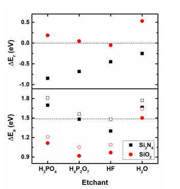
where ETS and Einit are total energies at the transition and initial states, respectively. Fig. 3 shows the reaction and activation energies for the two materials with four etchants. Si3N4 and SiO2 are very distinct in both reaction and activation energies. Lying below the dashed line (∆Er=0), H3PO4 and H4P2O7 etchants exothermically react with Si3N4, releasing energies of -0.85 and -0.69 eV per molecule, respectively. For SiO2, however, the reactions by both phosphoric acids are endothermic with at least larger than +0.05 eV.

Fig3
This subject was supported by the Global Frontier Program, through the Global Frontier Hybrid Interface Materials (GFHIM) (2013-M3A6B1078882). This work was also supported by the Technology Innovation Program (20011259, Development of Electrostatic Ceramic Heater Including Multizone Capable of Precision Temperature Control) funded by the Ministry of Trade, Industry & Energy (MOTIE, Korea).
上一篇: 湿蚀刻对HgCdTe表面性能的影响