In this paper, a comprehensive study of the etching behavior of this high selectivity etchant is presented, including the etch rate dependence of Si1-xGex (x = 0.2) on solution ageing time, and of the SiGe layer thickness (from 10 up to 60 nm) on the lateral solution etch kinetics of (Si1-xGex /Si) x3 multilayer. Several process parameters have been jointly studied such as etch rates, selectivity and collapse. we propose an innovative process SON enabling fabrication of the desired “super SOI” devices which are capable of quasitotal suppression and excellent electrical performances thanks to the extremely thin silicon (40 nm) and buried dielectric (10 to 60 nm) by using the simple HF:H2O2 :CH3COOH solution with a great selectivity.
The samples used for selective wet etching were grown by using reduced pressure chemical vapor deposition (RPCVD) system. The Si substrates were cleaned through a normal cleaning procedure (a hydrogen bake step to clear the surface from native oxide, performed at 1100℃) before the SiGe layer growth. The growth of the SiGe layer was then commenced by switching the SiH4 and GeH4 (1.5% diluted in H2 ) into reactor. The flow rates of SiH4 and GeH4 were changed from 10 to 100 sccm and from 40 to 300 sccm, respectively. The flow rate of H2 was fixed at 10slm. The growth temperature was 600℃ with a growth rate of 3.2 nm/min for the SiGe layer and a growth rate of 3.8nm/min for the Si layer. Finally, the layer structures were completed by depositing a 40 nm Si cap layer. The Ge concentration in the SiGe layers is 20%. The layer thicknesses and compositions were determined by TEM and EDX and showed excellent agreement with the nominal values. Fig. 1 shows the TEM image of the Si0.8Ge0.2 /Si multilayer grown by using RPCVD. The multilayer structure was consisted of a 10nm-thick Si0.8Ge0.2 layer, 40nm-thick Si layer, 40nm-thick Si0.8Ge0.2 layer, 40nm-thick Si layer, 60nm-thick Si0.8Ge0.2 layer, and 40nm-thick Si cap layer [23].
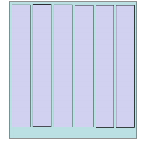
The samples were etched in a load-locked BMR (HiEtch) high-density plasma etching system consisting of an ICP chamber (operating at 2 MHz) and an additional RF bias (13.56 MHz) for the sample chuck. Helium back-side cooling was incorporated to allow the temperature of the substrate to be controlled more effectively. A CF4 gas with a purity of 99.999% was introduced for etching [24]. The schematic of dry etching patterning and generic sample structure used for selective wet etching is shown in Fig. 2.

Fig2
Previously, many studies has taken place using HF:H2O2 :H2O for the etching of Ge [27]. However, when this water-based diluents solution was used to etch Si1-x Gex , etch rates become lower. And it is evident that little change in the etch rate occurs with stirring and hence no etch rate or waiting time dependence on stirring could be seen for etching Si1-xGex in HF:H2O2 :H2O (1:2:3) [25]. As mentioned previously, this is to be expected due to the retarded oxidation of Ge in the presence of the Si atoms, which restrict etching. In this situation fewer Ge atoms are available for oxidation [25]. But the presence of the diluents CH3COOH changes the nature of the etching reaction. The etch rates are twice as high when using acetic acid instead of water. It is believed that the reaction between H2O2 and CH3COOH in the oxidation of the Ge atoms in Si1-x Gex is responsible for the waiting time and two plateau regions observed with this etchant.
This research was supported by Basic Science Research Program through the National Research Foundation of Korea (NRF) funded by the Ministry of Education (2009-0094031) and (Grant No. 2013R1A1A2010053). It was also supported by the Future Semiconductor Device Technology Development Program (Grant No. 10044651) funded By MOTIE (Ministry of Trade, Industry & Energy) and KSRC (Korea Semiconductor Research Consortium).
上一篇: MgO的湿法清洁
下一篇: SiO2在氢氟酸中的刻蚀机理