In this study, a novel wet etching technique for AlGaN/GaN heterostructures using dry thermal oxidation followed by wet alkali etching has been developed. It is demonstrated that a groove structure on an AlGaN/GaN heterostructure was formed. The etching step height was about 150 nm measured by atomic force microscopy (AFM).
A plot of the groove structures’ step heights and average roughness Ra of the wet-etched area measured by AFM with different oxidation times are shown in Fig. 1. The step heights are 129 nm, 147 nm, 150 nm, and 150 nm when the oxidation times are 2 h, 4 h, 6 h and 8 h, respectively. The 3D image of the groove structure of 8 h oxidation time is shown in Fig. 2. It is found that the step height increases nonlinearly with oxidation time and approaches to a saturation value. The topography of the wet-etched area also becomes better with longer oxidation time, where the average roughness Ra is 17.8 nm, 13.7 nm, 11.5 nm and 10.7 nm, respectively.
The TEM high resolution image of the AlGaN/GaN heterojunction structure after thermal annealing in pure O2 atmosphere at 900 ıC for 30 min is shown in Fig. 3. A 40 nm polycrystal layer which is different from the GaN single-crystal structure found in Fig. 3 should be an oxide layer, and similar results were observed that an oxide layer could be formed during high temperature oxidationŒ14; 15. Oxygen element distribution in the oxidation AlGaN/GaN heterojunction is shown in Fig. 4 as measured by EDS (energy diffraction spectrum). The oxygen element tends to disappear at 70 nm, about 40 nm away from the surface of the oxide layer, which could be thought of as the effective distribution depth of the oxygen element. The 40 nm oxygen element distribution depth is consistent with the thickness of the poly-crystal layer measured by TEM, which is clear evidence that the oxidation process occurs in the AlGaN/GaN structure under high temperature. The oxidation process could be described as follows. When the AlGaN/GaN wafer was exposed to the high-temperature O2 atmosphere, Al2O3 and Ga2O3 are formedŒ16, with the loss of the nitrogen. In Ref. Œ16, the oxidation process of the AlGaN layer was qualitatively schematized as:
2AlGaN C 3O2 , Al2O3CGa2O3 C N2 " : (1)
The oxidation process of GaN layer should be schematized as: 4GaN C 3O2 , 2Ga2O3 C 2N2 " : (2)

Fig1
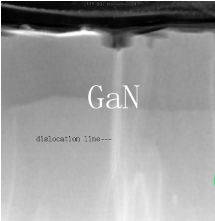
It is found that the wet-etching step height approaches saturation as oxidation time increases, as shown in Fig. 1. A possible explanation of the physical mechanism is given. During the high temperature oxidation, two processes co-exist: the diffusion of oxygen into the oxide/semiconductor interface and the reaction of O2 with the semiconductor. Usually, the defects were oxidized much more easily due to the much faster diffusion along the defects, resulting in a larger oxidation depth in the defects region. Thus, at the beginning, the roughness of the surface on the etched area was not good, as shown in Fig. 6 which is the cross profile of AlGaN/GaN heterostructure after thermal annealing for 30 min at 900 ıC in pure oxygen atmosphere followed by treatment in 70 ıC KOH solution. It is shown that there is a large etching depth on the dislocation region. However, as the oxide layer became thicker with longer oxidation time, the O2 diffusion through the oxide layer determines the oxidation rate. Thus when the generated oxide layer becomes thick enough to effectively hinder O2 diffusion to the oxide/semiconductor interface, the oxide depth reaches a saturation value, which results in better surface roughness, as shown in Fig. 1.
In summary, a novel wet etching technique for an AlGaN/GaN heterostructure based on thermal oxidation has been demonstrated and the physical mechanisms were also discussed. Our results showed that a poly-crystal oxide layer was formed under high temperature oxidation, and then could be wet-etched off by using KOH solution at 70 ıC. It is demonstrated that a groove structure with a step height of 150 nm was obtained using thermal oxidation at 900 ıC for 8 h in pure oxygen atmosphere followed by wet-etching in KOH solution at 70 ıC for 30 min. It is found that AlGaN/GaN heterojunction defects should accelerate the oxidization process, but the thickness of the generated oxide layer approaches saturation as the oxidation time increases, due to the thick oxide layer hindering oxygen diffusion to the oxide/semiconductor interface, which finally results in better surface roughness after adequate oxidation time.
上一篇: SiO2在氢氟酸中的刻蚀机理
下一篇: ZnO上 ZnCdO 的选择性湿法刻蚀