THE GaN-based wide bandgap semiconductors have attracted considerable interest, in terms of applications for optoelectronic devices, which operate in the blue, green, and ultraviolet UV wavelength regions, as well as for electronic devices operating at high-temperature/high-power conditions [1], [2]. However, owing to the large mismatch of lattice constant and thermal expansion between epitaxial GaN fifilms and sapphire substrates, high-density dislocations ranging from sapphire substrates, high-density dislocations ranging from cm degrade the light-emitting diode (LED) performance profoundly. Thus, growth of GaN with low-density dislocations has been a major effort for fabrication of reliable high-effificiency LEDs. By epitaxial lateral overgrowth (ELOG) with SiN or SiO mask patterned on as-grown GaN seed crystal, threading dislocations can be signifificantly eliminated [3]–[5]. Although this overgrowth technique can dramatically improve crystalline quality, the requirement of two-step growth procedure is time-consuming and easily introduced contaminations. Recently, the single-step growth on maskless patterned sapphire substrates (PSSs) has been widely proposed, and a comparable improvement of LED performance was demonstrated compared to the ELOG technique [6]–[10]. Though the single-step growth method cannot reduce the dislocation density to the order of magnitude that the ELOG technique can achieve cm [11], the simplifified technique shall be feasible for mass fabrication. Besides, geometrical shape of the sapphire patterns can effectively enhance light extraction effificiency by scattering or redirecting the guided-light inside an LED chip to fifind escaping cones [7], [10], [11]. Nevertheless, PSSs were generally fabricated by dry etching and it is unavoidable to damage the sapphire surface. In this letter, we report GaN-based LEDs grown on the chemical wet etching PSS, hence the sapphire surface damage induced by dry etching can be eliminated. Furthermore, the inclined crystallography-etched facet evolving on sapphire substrates with the etching time facilitates superior light extraction effificiency.
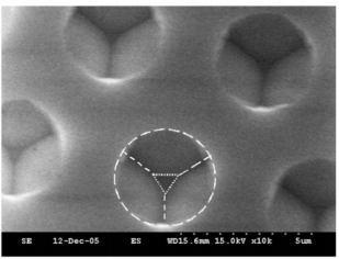
The GaN-based LEDs used in this study were grown using a low-pressure metal–organic chemical vapor deposition (Aixtron 2600 G) system onto -face (0001) 2 -diamerter patterned and conventional sapphire substrates. Fabrication of PSSs with inclined crystallography-etched facets was illustrated as follows: The SiO fifilm with hole-patterns of 3- m diameter and 3- m spacing was deposited onto the sapphire substrate by plasma-enhanced chemical vapor deposition and defifined by standard photolithography to serve as the wet etching mask. The sapphire substrate was then wet etched using an H PO -based solution at an etching temperature of 300 C. The sapphire wet-etching rate is about 1 m min in this study and can be related to the H PO composition and etching temperature [14]. Fig. 1(a) and (b) shows the top and cross section side views scanning electron microscope (SEM) images of the pattern sapphire substrate of the etching time of 90 s. In Fig. 1(a), the crystallography-etched pattern of an (0001)-oriented sapphire substrate has a flflat-surface of {0001} -plane with triangle-shape in the center. Surrounding the triangle-shape -plane are three facets of {1-102} -plane with an angle of 57 against [0001] -axis.

Fig1
Fig. 3(a) shows measurement results of room temperature output power ( – curve) and external quantum effificiency of conventional and PSS LEDs as a function of the forward-bias current. The data were obtained from the same fabrication process with and without crystallography-etched patterns on the sapphire substrate, explaining why any factor causing this difference except the patterned sapphire would be neglected. The light output powers at 20 mA of the conventional and PSS LEDs without epoxy resin are 7.8 and 9 mW, respectively, i.e., an improvement factor of approximate to 1.15 was achieved by adopting the sapphire substrate with crystallography-etched facet patterns.
High light-extraction-effificiency GaN-based LEDs were successfully grown on PSSs fabricated by chemical wet etching. The output power is increased by approximately 15% on the PSS LED compared with the conventional one at an injection current of 20 mA. The improvement was attributed not only to the geometrical shape of {1-102} crystallography-etched facets that effificiently redirects the trapped light to fifind escape cones, but also to dislocation density reduction by adopting the PSS growth scheme.
上一篇: ZnO上 ZnCdO 的选择性湿法刻蚀
下一篇: 晶圆湿法清洗的速率检测器