In semiconductor substrate (wafer) cleaning, wet cleaning is essential. Wet cleaning may include both chemi cal and mechanical means for wet etching thin film layers and/or removing particles on a wafer Surface. In the current State of art, one means of wet cleaning includes the use of an acoustic energy cleaning device. An acoustic energy cleaning device utilizes a proceSS wherein a wafer is placed in a liquid bath and high frequency irradiation, or cavitation, is applied to the liquid in the bath. At the same time, chemicals in the liquid provide a Surface etching to layers on the wafer. The Surface etching and cavitation together pro vide mechanical and chemical actions that clean the wafer Surface.
The batch process, however, suffers from various problems. For example, the batch process is timely. The various Steps of etching the wafer, removing the wafer from the liquid bath, measuring the wafer, and repeating the etch take valuable time. The batch proceSS is clumsy and ineffi cient. The wafer has to be moved around leading to potential risks of damaging delicate portions of the wafer. The batch proceSS is imprecise. The timing of each cleaning etch can only be estimated and cleaning etch results can only be verified by removing the wafer from the bath to make measurementS.
Described herein is a rate monitor for wet wafer cleaning. In the following description numerous specific details are set forth. One of ordinary skill in the art, however, will appreciate that these specific details are not necessary to practice embodiments of the invention. While certain exem plary embodiments of the invention are described and shown in the accompanying drawings, it is to be understood that Such embodiments are merely illustrative and not restrictive of the current invention, and that this invention is not restricted to the Specific constructions and arrangements shown and described since modifications may occur to those ordinarily skilled in the art.
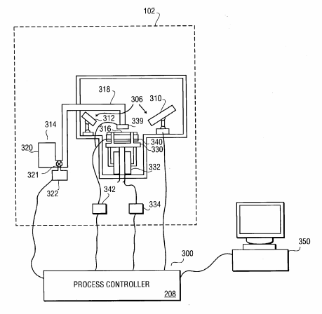
FIG. 1 illustrates a wet cleaning system according to one embodiment of the invention. Referring to FIG. 1, the wet cleaning System includes a Single-wafer cleaning device 102 and a rate monitor 104 connected to the single-wafer cleaning device 102. The single-wafer cleaning device 102 is to provide a wet cleaning etch, and other cleaning pro cesses, to a wafer. The term "wafer', as defined herein, may encompass Semiconducting materials, non-conducting mate rials, or combinations of Semiconducting and non-conduct ing materials. The wafer includes a Substrate comprising any one of various Substrate materials known in the art, Such as monocrystalline Silicon. The wafer may also include Struc tures and devices that have one or more insulative, Semi insulative, conductive, or Semiconductive layerS and mate rials. According to one embodiment of the invention, the Single-wafer cleaning device 102 is a Single-wafer cleaning device as described in further detail in conjunction with FIGS. 3, 4, and 5A-5F below.

Fig3
Described herein is a rate monitor for wet wafer cleaning. In the following description numerous specific details are set forth. One of ordinary skill in the art, however, will appreciate that these specific details are not necessary to practice embodiments of the invention. While certain exem plary embodiments of the invention are described and shown in the accompanying drawings, it is to be understood that Such embodiments are merely illustrative and not restrictive of the current invention, and that this invention is not restricted to the Specific constructions and arrangements shown and described since modifications may occur to those ordinarily skilled in the art..
下一篇: 硅薄膜太阳能电池的铝薄膜