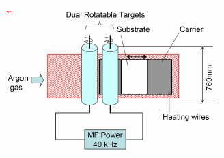
The thicknesses of ZnO:Al thin films are tested with surface profiler with the accuracy of 10 nm ( Dektak 3030, Veeco Instruments Inc). The electrical properties of ZnO:Al thin films were characterized by Hall effect measurements. Diffuse and total transmissions (DT and TT) as well as total reflection (TR) and the absorption of ZnO:Al thin films were measured by a double-beam spectrophotometer with an integrating sphere (Perkin Elmer Lambda 19). In order to avoid the test error by the rough surface structures, the index matching liquid (CH2I2) was used during the TT and TR measurements [12]. The topographies of the samples were investigated by scanning electron microscopy (SEM, Supra 55VP SmartSEMTM, Carl Zeiss, Germany). The chemical compositions of sputtered ZnO:Al films were characterized by secondary ion mass spectroscopy (SIMS). The current-voltage (I-V) parameters of silicon thin films solar cells were measured with the sun simulator (WACOM-WXS-140S-Super) under the standard tested conditions (1000 W/m2 , AM1.5, 25C).
Fig. 2 shows the dynamic deposition rates (DDRs) of ZnO:Al films deposited at different substrate temperatures and discharge powers as well as different working pressures (1.0 Pa and 1.5 Pa). ZnO:Al films deposited at a specific discharge power and different substrate temperatures show similar DDRs. It is also found that the DDR almost linearly increases from approximate 11 nmm/min up to 90 nmm/min with the enhanced discharge power from 2 kW to 14 kW. The thicknesses of all films are kept between 800 nm and 1000 nm. The normalized DDR is about 6 nmm /(minkW) here. Kim et al.[13] reported that the deposition rate decreased with the increasing substrate temperature due to thermal desorption of adatoms from substrate surface. However, such a kind of observation did not happen here, which could be due to the relatively higher working pressures (1.0 Pa and 1.5 Pa) compared to the working pressure of 2 mTorr ( is approximately equal to 0.26 Pa) used in the reference [13]. Even though the substrate temperature seems not to strongly effect on the deposition rate, it leads to different electrical properties and grain structures as well as etching behaviors.

Fig2
The dependence of carrier mobility () of ZnO:Al films on substrate temperature is given in Fig. 3(c). The mobility increases with the enhanced substrate temperature. Highest mobility of up to 50 cm 2 /Vs was achieved for low rate films deposited at 2 kW. Even for high rate films deposited at 14 kW, a high mobility of about 45 cm 2 /Vs was obtained. It is a great advantage for such a kind of sputtering technique. The high substrate temperature leads to a high crystallizations of polycrystalline ZnO:Al films and then reduces the scattering of carrier (electron) at the grain boundaries [16-18]. Moreover, the hall mobility is expected to reduce when the substrate temperatures increases to an even higher temperature. Since high substrate temperatures could lead to the strong a re-evaporation of zinc atoms as well as the formation of alumina, which works as local defects and then results in the decrease of hall mobility [14, 15, 19-21]. In addition, the tensile stresses at high substrate temperatures, which are usually caused by grain boundary relaxation [22, 23], could be dominated compared to the compress stresses.
As pointed out above, the etching behaviors are strongly related with the grain structures. However, it is not clear about the exact relationship between them so far. Maki et al. [31] studied the chemical wet behaviors on single crystal ZnO (001) polar surfaces i.e. Zn-terminal surface and O-terminal surface. After etching in HCl solution, the hexagonal pit shape formed. In fact, Hüpkes et al. also reported different surface structures by etching single crystal ZnO from Zn-terminal surface and O-terminal surface [32, 33]. However, for polycrystalline ZnO:Al the etching behavior is much more complex. Different deposition conditions lead to the formation of different surface textures after the chemical wet etching treatment.
上一篇: 晶圆湿法清洗的速率检测器