A novel system has been developed for evaluating thinfilm oxide semiconductors using a μ-PCD (Microwave Photo Conductivity Decay) method. Variations of the mobility and Vth shift are issues in the manufacturing process of oxide semiconductors. To resolve these issues, an evaluation technique has been established. In addition, the mura (unevenness) of film quality on substrate has become another issue as the substrate size increases. It has been demonstrated that mapping measurement is effective in resolving this issue.
With the prevalence of smartphones and tablets, flat panel displays (FPD) are required to have higher definition, increased display frequency and lower power consumption. Thin-film transistors (TFTs) using oxide semiconductors, as typified by In-GaZn-O (IGZO)1) , have mobilities higher than those of conventionally used amorphous Si (a-Si), making higher definition possible. Additionally, the FPD manufacturing lines for IGZO also allow lines for a-Si to be used with almost no alteration. Therefore, there are an increasing number of compact panels using oxide semiconductors. Their demand for such panels for large-sized television sets is also expected to increase in the future.
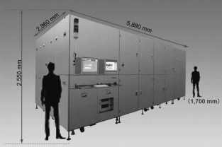
Fig. 1 shows an example of the systems developed: the μ-PCD measurement system (LTA- 2850SPHIIB) for generation-8.5 LCD (G8.5: substrate size, 2,200×2,500mm). This system has a depth of 5,880mm, width of 2,860mm and height of 2,550mm. The current lineup covers the range from research and development application (substrate size: 200×200mm) to the G8.5 substrate size.
With the substrate size increased, if the conventional system is used, the measurement time will increase. Therefore, the systems for G5.5 or larger sizes use a dual-head method involving two measurement heads. Fig. 2 shows the configurations of a conventional single head and newly designed dual head. In each configuration, the stage moves in the X-axis direction, while the head is/heads are moving in the Y-axis direction. The dual-head configuration halves the amount of movement in the Y-axis direction, shortening the measurement time for a G8.5 substrate, from the approximate 40 minutes it used to take, to 20 minutes or less.

Fig1
When an oxide semiconductor thin film is irradiated with laser energy exceeding the energy bandgap, electron-hole pairs are generated and excess carriers are produced. These excess carriers are annihilated by recombination, and the time it takes to annihilate them (lifetime) depends on the physical properties of the samples. The excess carriers generated by laser irradiation increase the conductivity of the sample, changing the microwave reflectivity (Fig. 3). The μ-PCD is a method of measuring lifetime from the temporal change in the microwave reflectivity.
上一篇: 湿蚀刻法制备的LiNbO3
下一篇: 硝酸浓度对多孔氧化锌薄膜刻蚀工艺能的影响