Widespread deployment of solar photovoltaics (PVs) is crucial to meeting the world’s growing energy demand and mitigating climate change in the future; however, solar PVs remains expensive and unreliable compared with methods, such as fossil fuel-based electricity generation.It is widely accepted that low-cost high-efficiency solar PVs capture more solar energy and make solar energy economically competitive with fossil fuels. In the past decades, crystalline siliconbased PVs dominated commercial PVs owing to their low-cost, earth-abundance, and reliability; however, the poor infrared absorption owing to its indirect bandgap, as well as the high reflectivity resulting from surface texturing processes, hurts the cell efficiency, and hence poses a daunting challenge to the large-scale deployment of silicon-based PV modules.[8,9] Furthermore, new ideas striving for more efficient utilization of sunlight have also been under development.A promising high-efficiency silicon PV technology is the use of black silicon (b-Si) solar cells, which are based on crystalline silicon (c-Si) wafers with micro/nanostructured surfaces that appear black to human eyes because it can efficiently capture sunlight across a broad range of wavelengths and angles of incidence. The excellent light trapping capability of b-Si allows significant reduction in wafer thickness even without the application of an antireflection coating; hence, it is a promising material candidate for cost-efficient silicon PVs.
The fabrication of luminescent porous silicon by metal enhanced silicon etching was first demonstrated by Zhang et al. in 1993. They produced a porous silicon layer on an n-type silicon polished surface when the n-silicon in contact with a gold was illuminated in an HF solution containing oxygen without an externally applied potential. In 1997, Dimova-Malinovska et al. reported the fabrication of porous silicon by etching an aluminum coated silicon substrate in an HF–HNO3 aqueous solution. They claimed that the incubation time necessary for the formation of porous silicon was decreased dramatically owing to the presence of the Al film. In 1999, inspired by the discovery of Zhang et al., Kelly et al. demonstrated that a luminescent porous silicon layer can be made on p-type silicon surface in a similar manner without illumination. In their experiment, as shown in Figure 2a, a silicon wafer was short-circuited to an inert metal by evaporating an inert Au/Cr film onto the back side of the wafer, thus forming a galvanic cell. The resulting porous silicon layer with a thickness of 7 µm is shown in Figure 2b. They proposed that the porous silicon is obtained by galvanic etching owing to the formation of metal/silicon galvanic cells in which the silicon acts as anode and metal as cathode in oxidizing HF aqueous solutions. The galvanic etch rate can be controlled by the metal/silicon area ratio and oxidant concentration of the HF solutions.
It is desirable to move vertical SiNW arrays from silicon substrates to a different substrate, such as a flexible one for flexible devices. Weisse and Zheng et al. report an exciting and simple method to vertically transfer SiNW arrays with uniform length onto different substrates by creating horizontal crack in the SiNWs. The crack is formed by soaking an Ag-MacEtch SiNWs sample in water and the subsequent Ag-assisted etching processes of SiNW arrays, as shown in Figure 5. The authors suggested that the crack formation is related to the delamination and reattachment of an Ag film during water soaking; however, this simple water-soaking crack method does not work for the delamination and reattachment of gold film. The crack method facilitates embedding SiNWs within polymers and integrating SiNWs into channels, thereby enabling the realization of vertical SiNW devices that are mechanically flexible and scalable to large dimensions.

Fig2(a)
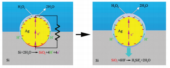
Silicon dissolution during the MacEtch of silicon in HF solutions consisting of divalent and tetravalent dissolution processes was proposed on the basis of experimental results, and the two half-cell reactions that include cathodic and anodic reactions are expressed in the following equations (Equations (1–4)). The additional cathodic reaction expected to occur on the metal or silicon surface is the reduction of noble metal ions since their metallic form may dissolve in the oxidizing HF solution, while the strong oxidizing solution environment does not favor the cathodic reduction of hydrogen ions. Clearly, besides the localized silicon dissolution at the metal–silicon interface, the overall electrochemical reactions involved in MacEtch of silicon are identical to those in electrochemical etching or stain etching of silicon in HF aqueous solution containing strong oxidants.
下一篇: 硅基质上残留超纯水滴留下干燥缺陷研究