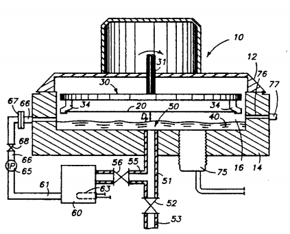
Disclosed are methods and apparatuses for combined etching and cleaning of semiconductor wafers and the like preferably using hydrofluoric acid (HF), hydro chloric acid (HCl) and water solutions which generate equilibrium vapor mixtures of HF vapor, HCl vapor and water vapor as a homogenous processing gas. The processing gases do not employ a carrier gas which will make the vapors nonhomogeneous and reduce etching rates. The vapors are preferably generated from a liquid source which is provided within a contained reaction chamber which holds the wafer. The wafer is prefera bly oriented with the surface being processed directed downward. The wafer is advantageously positioned above or in close proximity to the liquid source of the processing vapor. The wafer is rotated at a rotational speed in the range of 20-1000 revolutions per minute to provide uniform dispersion of the homogeneous pro cessing gas across the wafer surface and to facilitate circulation and transfer from the liquid source into pro cessing gas and onto the processed surface. The liquid source of the vapor can advantageously be provided in a bath immediately below the processed surface of the wafer or in toroidal basin adjacent to the wafer. The processes provide high speed etching of good unifor mity and superior particle count performance.
It is common in the processing of silicon wafers to remove or etch portions of a layer of silicon dioxide using an etchant. A common etchant is hydrofluoric acid. This is typically done using an immersion process wherein a wafer, or one or more carriers containing a number of wafers, is immersed in the desired hydroflu oric acid containing processing fluid.
One of the disadvantages of immersion etching pro cesses is that the wafers typically exhibit an increase in the numbers of particulates which become adhered to or imbedded in the wafer. As the feature size of semi conductor wafers continues to decrease into the sub micron sizes, now typically in the range of 0.1-0.5 mi cron, the need for minimizing contamination becomes more acute. These small feature sizes also create addi tional problems for immersion processing because sur face tension effects can reduce etching uniformity and resulting product quality.
It has previously been recognized that silicon wafers can be processed by using etchant gases, including gases which contain hydrofluoric acid (HF). In an article entitled, "Etching of Thin SiO2 Layers Using Wet HF Gas' authors P. A. M. van der Heide et al., describe the etching of silicon dioxide layers by using vapor mix tures of HF, water and nitrogen. The article describes using a flow of nitrogen carrier gas through a vessel containing a 10% hydrofluoric aqueous solution. The nitrogen carrier produced a flow of etchant gas which was directed through a nozzle against the surface of a small silicon wafer being etched. A flow of dry nitrogen was passed over the opposite side of the wafer to reduce the effects of ambient atmospheric water which was present in the essentially open atmospheric process. Temperatures from 25'-40' C. were indicated for the HF solution and from 25 C. to about 60' C. for the wafer. The authors also reported that high temperature treatment under vacuum conditions foll.

Fig1
One deficiency of the process described is the contin uation of etching after the process exposure has begun. This results in uneven etching rates and problems in the resulting integrated circuit devices due to variations in feature sizes across the device. The etching uniformity is also deficient in that the process arrangement may not provide assurance of equilibrium homogeneous presen tation of the reactant gas to the wafer being processed. Variations in the uptake of the vapors by the incoming carrier gas stream can result in instantaneous variations in the etchant gas stream which can affect processing.
A deficiency of both of the above processes is the relatively poor ability of these techniques in removing metallic ions or other metallic contaminants which may exist either as impurities in the oxide layer or as particu late contaminants which have adhered to the surface of the wafer. It is now common to use a series of cleaning processes after etching of silicon wafers. Dilute hydro fluoric acid treatment followed by processing in water, hydrogen peroxide and annonium hydroxide is a con mon cleaning approach. This is typically followed by processing in water, hydrogen peroxide and hydrochlo ric acid to further clean the wafers. These cleaning processes are in addition to prior HF etching. Such a series of processing steps is time-consuming and adds to product cost.
Prior of this invention there has been a long-felt need in the art for one-step processing which will provide uniform and repeatable etching results while achieving low contamination rates and cleaning of metallic ions and other metallic impurities and particulates. Other objectives and advantages of the invention are also indicated herein.
上一篇: 光刻胶回流特性在金刚石微透镜制造中的应用
下一篇: 薄膜有机光伏电池中使用微透镜捕获光