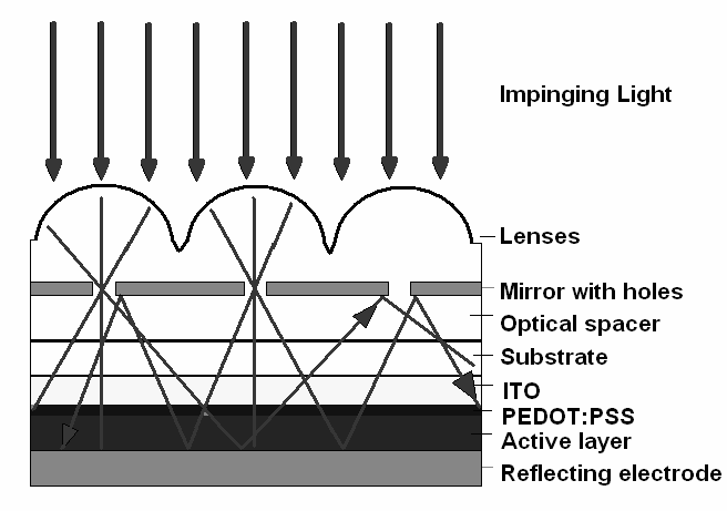
Abstract: We demonstrate a novel light trapping configuration based on an array of micro lenses in conjunction with a self aligned array of micro apertures located in a highly reflecting mirror. When locating the light trapping element, that displays strong directional asymmetric transmission, in front of thin film organic photovoltaic cells, an increase in cell absorption is obtained. By recycling reflected photons that otherwise would be lost, thinner films with more beneficial electrical properties can effectively be deployed. The light trapping element enhances the absorption rate of the solar cell and increases the photocurrent by as much as 25%.
A promising material class for manufacturing inexpensive photovoltaic cells is comprised of blends of conjugated polymers and fullerenes [1, 2]. These organic blends are sandwiched between transparent and reflective electrodes, and are typically 50-300 nm thick. The power conversion efficiency (PCE) of organic solar cells (OSC) is however still limited and they do not perform as well as their inorganic counterpart. One limitation of OSCs is the low charge carrier mobility which prevents generated charges from reaching the electrodes. Film thickness minimization is therefore a route to collect a larger fraction of the photo generated carriers, but a minimum thickness is always required for sufficient photon absorption. If the absorber is too thin, the device will simply reflect most impinging light. In this work we show how to construct and incorporate novel light trapping structures that enable higher photon absorption in a thin film by recycling the reflected photons.
Light trapping in thicker inorganic photovoltaic cells is a well known approach to increase the photocurrent . In such cells the trapping of light is fulfilled by the introduction of a rough or structured active layer. As photons hit the structured features of the cell, they are forced to travel more in the plane of the absorber rather than perpendicular to it. As an efficient light scattering element should be somewhat larger than the wavelength of light to effectively alter the photon propagation direction, difficulties are inherent when incorporating such refractive or reflective structures inside a ~100 nm thick organic film. The electrical properties are extremely limiting when including light scattering elements in direct contact with such thin active layers. Therefore, different engineering solutions may be required, where the light trapping element is separated from the thin active layer and thereby allow for beneficial scattering but avoid the possibility of electrical defects.

Fig1
The light trap is initially placed in front of an integrating sphere and the transmission in the forward and backward directions is characterized. Fig 4(a) shows the trap transmission as a function of wavelength. A strong asymmetry between the forward and backward transmission was confirmed, with transmission ≤ 90% in the forward direction (first through lenses and then mirror) and <15% measured with the sample illuminated from the side of the mirror. We observe that high forward transmission, obtained without the use of antireflection coatings or moth-eye structures, could be achieved only with the full surface coverage with micro lenses (Fig. 3), made possible by the present fabrication process. The dip in transmission at shorter wavelength is attributed to absorption in the lens material as well as in the metal mirror.
The active bulk heterojunction consists of a 1:3 ratio blend of the low band gap alternating polyfluorene APFO Green-9 and the soluble fullerene derivative PCBM whose molecular structures are inset in Fig. 4(b). The active layer in this device is spin coated from a 7 mg/ml chloroform solution at a speed of 3000 rpm. The layer thickness is only 30 nm, and has therefore a limited absorption. The reflection (R) from an operational solar cell with an area of 1.3 cm2 is measured and the corresponding device absorptance (1-R) together with the active layer absorption is presented in Fig 4(b).
The photoresponsivity (PR) from the thin solar cells, measured with and without the light trap laminated to the device, is presented in Fig. 5(a). The irradiance of the AM 1.5 solar illumination spectra is inset as a comparison. As can be seen from the PR curve, the light trap works very effectively over a broad spectral range. For this material and thickness, light trapping is beneficial for all wavelengths longer than 450 nm. The loss of the high energy photons is no major concern as their abundance is rather limited simultaneously as their energy may actually be harmful for the stability of the active polymer. The current/voltage curve (Fig. 5(b)) under AM 1.5 simulated solar illumination also demonstrate an increase in short circuit current, as high as 25%, upon the inclusion of the light trap.
上一篇: 半导体晶片的氢氟酸和盐酸蒸汽处理