Abstract: Wafer-level packaging (WLP) based camera module production has attracted widespread industrial interest because it offffers high production effiffifficiency and compact modules. However, suppressing the surface Fresnel reflflection losses is challenging for wafer-level microlens arrays. Traditional dielectric antireflflection (AR) coatings can cause wafer warpage and coating fractures during wafer lens coating and reflflow. In this paper, we present the fabrication of a multiscale functional structure-based wafer-level lens array incorporating moth-eye nanostructures for AR effffects, hundred-micrometer-level aspherical lenses for camera imaging, and a wafer-level substrate for wafer assembly. The proposed fabrication process includes manufacturing a wafer lens array metal mold using ultraprecise machining, chemically generating a nanopore array layer, and replicating the multiscale wafer lens array using ultraviolet nanoimprint lithography. A 50-mm-diameter wafer lens array is fabricated containing 437 accurate aspherical microlenses with diameters of 1.0 mm; each lens surface possesses nanostructures with an average period of ~120 nm. The microlens quality is suffiffifficient for imaging in terms of profifile accuracy and roughness. Compared to lenses without AR nanostructures, the transmittance of the fabricated multiscale lens is increased by ~3% under wavelengths of 400–750 nm. This research provides a foundation for the high-throughput and low-cost industrial application of wafer-level arrays with AR nanostructures.
The production of micro camera modules for mobile phones and other Internet of Things (IOT) terminals has developed into a large market. Although micro camera module production is mainly accomplished by the vertical assembly of discrete lenses, the wafer-level packaging (WLP) approach for micro cameras has attracted widespread attention because it offffers compact module sizes and high production effiffifficiency . In the WLP process, several wafer-level dense microlens array plates are vertically assembled after wafer-scale registration, and then cut into thousands of discrete micro camera modules. The resulting camera module is a compact cube free of the traditional lens housing components. The wafer-level dense microlens array is the core component for WLP production. However, suppressing the ~4% Fresnel reflflection of wafer-level microlens arrays to <1% remains a major challenge. The traditional approach uses antireflflection (AR) coatings deposited on the surfaces of the lenses, such as quarter-wavelength multilayer dielectric coatings . However, the wafer-level microlens array of 4–8 inches in diameter has a low thickness of several hundred micrometers, which yields a high probability of wafer warpage during coating deposition. Wafer warpage can seriously damage wafer registration. Moreover, micro camera modules must withstand high-temperature reflflow processes during the process of welding onto circuit boards. Dielectric AR coatings can rarely survive such processes, because their thermal expansion coeffiffifficient mismatches with the base microlens material, and can cause coating fracture . These factors indicate that wafer-level microlens array production requires new AR solutions.
The moth-eye nanostructured surface is characterized by a uniform layer of quasi-periodical protuberances on a substrate . The lateral period of the nanostructures is much smaller than the optical wavelengths and is thus equivalent to a diffffraction grating where only the zeroth order can propagate, while all other orders are evanescent . The moth-eye layer is optically equivalent to a fifilm with a refractive index gradient in its depth direction , rather than the abrupt change in index that occurs in fifilms without nanostructures. Figure 1a shows schematically the continuous increase of the physical thickness of the nanostructures along the AR structured surface from air to the bulk. The moth-eye nanostructure can thus be modeled as a multilayer system with difffferent effffective refractive indices.
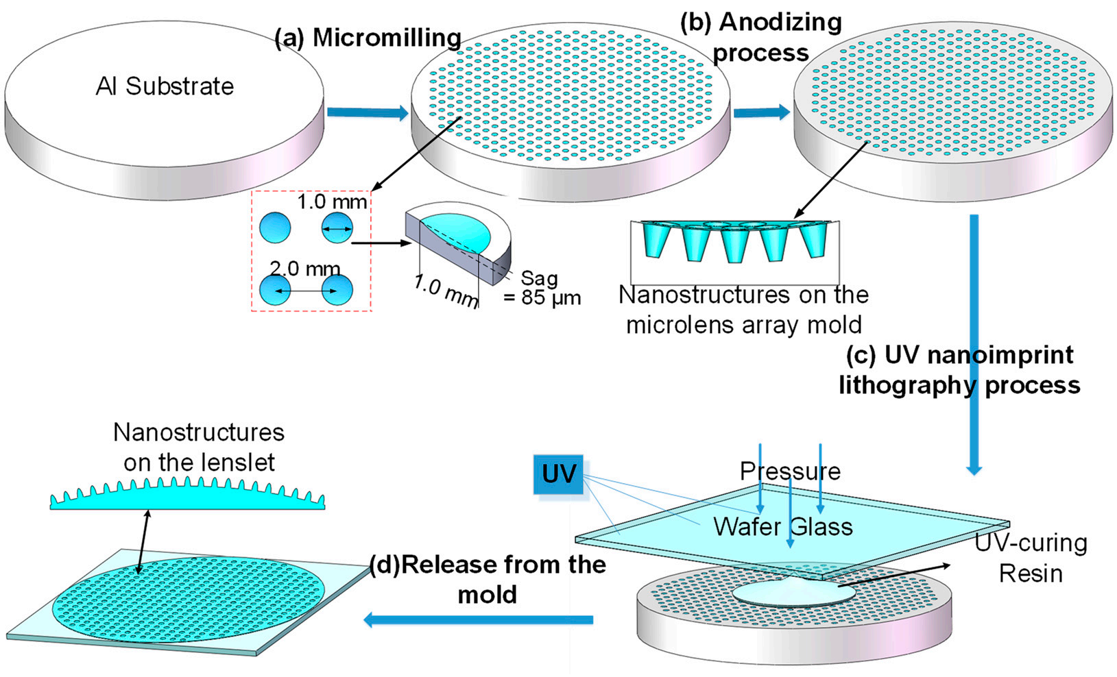
The process for producing AR nanostructures on the wafer-level lens array is depicted in Figure 3. Firstly, a 4–8-inch-diameter (10–20.3-cm-diameter) aluminum plate, with the diameter matching the targeted wafer lens array size, was manufactured into a high-precision wafer-level lens array mold using a diamond milling machine according to the design of the microlens surface. The microlens surface could be spherical, aspheric, or free-form in shape . Secondly, the metal mold was treated using a chemical approach to create an even layer of V-shaped nanopores on the hard mold . Next, a UV-curable resin-based nanoimprint process was used to transfer the hybrid structures on the metal mold to a glass wafer substrate, generating the wafer lens array with nanostructured surfaces. Finally, the wafer-level lens array was released from the mold after curing. To achieve a concave microlens array, the above wafer lens array could serve as an intermediate mold; another nanoimprinting process with steps similar to the one mentioned above could be performed to deposit the array on a curved substrate. This process matches well with the current, mainstream wafer lens array manufacturing process, and therefore, has a high probability of industrial applicability.

Fig1
The fabrication of the wafer-level lens array mold with hybrid structures was the most critical step of the process. Wafer-level microlens arrays have very high dimensional accuracy requirements for the profiles and positioning of the lens. To meet these requirements, the dense microlens array mold was fabricated on an ultraprecise machine (350FG, Moore Nanotechnology, Swanzey, NH, USA) with five-axis servo motion. After numerous trials to identify the right material, such as singlecrystal versus polycrystalline pure aluminum, and different aluminum alloys, an aluminum alloy (6061) substrate electroplated with ~0.3-mm-thick pure aluminum comprising nanosized grains (AlumiPlate, Coon Rapids, MN, USA) was finally selected as the mold material. This was done by considering the requirements of both the ultraprecise machining process and the subsequent chemical AAO process. A diamond turning process was used to create an optically flat surface on the 50-mm-diameter aluminum substrate, as shown in Figure 4a. Next, a concave and dense microlens array was machined by a micro-milling process using a high-speed air-bearing spindle, as shown in Figure 4b. The resulting wafer mold contained 437 accurate aspherical lens mold cavities with a cavity aperture of precisely 1.0 mm and a sag of 85 μm. The surface roughness (Sa) of the resu.
下一篇: 通过旋涂工艺在金刚石上制造凹面微透镜