Wide bandgap semiconductor materials A3 N and their alloys have a set of unique electrical, optical and mechanical properties, which are important in modern optoelecronics, high power electronics and microelectromechanical systems (MEMS) industry. Since natural substrates for A3 N materials are very expensive, silicon carbide (SiC), sapphire (c-Al2O3) and silicon (Si(111)) substrates are used for epitaxial growth of III-nitrides.
Crystallographic polarity is an essential feature of nitride semiconductor materials with wurtzite crystal structure. Polarity affects the growth kinetics, chemical, structural, optical and electrical properties of heterostructures . N-polar A3 N films are chemically active, while metal-polar layers, which are used more often, are known to be almost chemically inert. Thus the post-growth treatment of metal-polar nitrides by wet chemical etching is challenging. But it can be an advantage for MEMS production. Sacrificial layers are always used to from MEMS. This step can be skipped when etching of the substrate by solution to which the nitride layer is resistant.
In this work the experiments for investigation the effects of H3PO4:CH3COOH:HNO3:HF etching solution, taken with different concentrations, to the GaN/SixNy/Si(111) epitaxial structures were carried out. The aim of the experiments was at least partial separation of GaN epitaxial layer from the Si(111) substrate. The Ga-polar GaN films of 0.6-0.8 mkm thickness were obtained by plasma assisted molecular beam epitaxy (PA-MBE) on Veeco Gen 200 MBE system equipped with RF plasma source. The layers were grown on the semi-insulating (R > 10 kΩcm) Si(111) substrates, which were cleaned according to the Shiraki method. Before the growth, the Si(111) substrates were annealed at Tsub = 850 °C and then nitridated in the growth chamber using different nitridation temperatures and times. Thin SixNy layer, formed during the nitridation process, was used as a buffer layer.
To identify crystallographic polarity of the samples obtained the express-technique was developed (patent application №2016144845 15.11.2016). The meaning of developed technique is the observation of the surface morphology modifications as a result of anisotropic wet chemical etching by hot aqueous KOH solution in case of N-face structure, while surface and thickness of Ga-face material remain unchanged. Checking for surface morphology changes was carried out using scanning electron microscope 25 Supra Zeiss.

Fig1
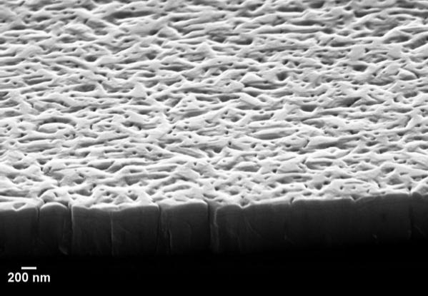
Despite the Ga-polarity, some changes in the surface morphology of the sample (hexagonal etch pits) are clearly visible (see figure 1, b). The primary cause of their appearance can be selective etching of various structural defects present in the GaN epitaxial layer: dislocations , nanotubes or inversion domains . However, the morphology of the defect-free areas and the thickness of the epitaxial layer remained unchanged, that indicates the Ga-polarity of the sample.
The H3PO4:CH3COOH:HNO3:HF etching solution includes a mixture of nitric and hydrofluoric acids, which is commonly used for silicon etching. Therefore the separation mechanism of the GaN film from the SixNy/Si(111) substrate is based on the silicon etching. However it should be noted that the etching occurs on the GaN/Si interface (see figure 3). Wherein, thin SixNy layer dissolves completely, as it was confirmed by additional experiments.
上一篇: 各种薄膜颗粒有效湿清洗方法的评价