Abstract—The InGaN-based light-emitting diodes (LEDs) with a roughened backside on the N-face surface of GaN substrate were fabricated through a chemical wet-etching process to increase light-extraction effificiency. The stable crystallographic etching planes were formed as the GaN planes. When the near-ultraviolet and blue LED were operated as a forward current of 20 mA, the output power of LEDs was improved from 13.2 and 19.9 mW to 25.6 and 24.0 mW, respectively. The different enhanced ratio is attributed to the different transmittance as a function of wavelength is caused from hexagonal pyramid on N-face GaN substrate after wet-etching process.
RECENTLY, tremendous progress has been achieved in GaN-based blue, green and ultraviolet light emitting diodes (LEDs). These nitride-based LEDs are also potentially useful for solid-state lighting. To realize solid-state lighting, however, one needs to further improve output ef- fificiency of these LEDs. It is known that light-extraction effificiency of GaN-based LED is limited mainly by the large difference in refractive index between GaN fifilm and the surrounding air. The critical angle for photons to escape from GaN fifilm is determined by Snell’s law. The angle is crucially important for the light-extraction effificiency of LEDs. Since the refractive indexes of GaN and air are 2.5 and 1, respectively, external quantum effificiency was limited to only a few percents for conventional GaN-based LEDs. It has been demonstrated that several methods can be used to improve light-extraction effificiency in InGaN-based LEDs on Al O substrate, such as bottom patterned Al O substrate [3], top p-type GaN:Mg rough surface processes , the formation of photonic crystal structure and selective oxidization on the mesa sidewall through a photoelectrochemical (PEC) wet oxidation process . Among these, PEC etching has advantages in terms of the compatibility with conventional semiconductor processing equipment and easy scalability to large wafers as well as the processing cost.
H. M. Ng et al. have reported the formation of GaN nanotip pyramids by selective and anisotropic etching of N-polar GaN in Potassium Hydroxide (KOH) solution . An aggregation of hexagonal pyramids with defifined facets and very sharp tips were formed. A similar concept could also be applied to the applications of GaN substrate. In other words, we might be able to enhance the LED output power by textured backside of the LEDs. In this study, InGaN-based near-ultraviolet (n-UV) and blue LEDs were grown on GaN substrate, respectively. Detailed fabrication process, numerical demonstrations, and the properties of fabricated LEDs will also be discussed.
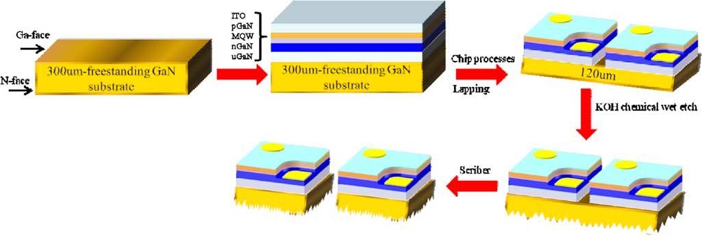
The n-UV and blue InGaN/GaN LEDs used in this study were all grown on c-face 2-inch GaN substrates in a SR-4000 atmospheric pressure metal–organic chemical vapor deposition system. GaN substrates were fabricated by C. L. Chao et al. group. LED structure consists of a 4- m-thick Si-doped GaN n-cladding layer, an multi quantum well (MQW) active layer, a 20-nm-thick p-type Mg-doped Al Ga N layer and a 200-nm-thick Mg-doped GaN layer. The MQW active region consists of fifive periods of 2.4-nm-thick undoped In Ga N well layer and 9-nm-thick undoped GaN barrier layer. During the MQW growth, the growth temperature was modulated in order to adjust the peak wavelength of LED. The peak wavelength of these n-UV and blue LED was 405 and 450 nm, respectively. For the fabrication of LEDs, indium tin oxide (ITO) was fifirst deposited on these LEDs as a transparent contact layer (TCL). Then, we partially etched the surface of the samples until the n-type GaN layers were exposed. We subsequently deposited Cr/Au onto the exposed n-type and p-type GaN layer to serve as the n-type and p-type electrode. The chip size of LEDs was 375 m x375 m.

Fig1
In order to understand the surface texture how to inflfluence the light extraction effificiency, transmission measurements (Perkin Elmer spectrometer, Lambda 40) was performed. Fig. 3 shows the transmission spectra as a function of wavelength from Ga-face GaN substrate after chemical wet-etching process with various etching times. These measured transmittance samples of sample I, II, IV and V are the same as that of SEM measurement, as shown in Fig. 3. The transmission intensity is relative value. Fig. 3(a) is transmittance of GaN substrate without chemical wet-etching process. It was found that the transmittance at 405 nm wavelength is lower than 450 nm wavelength. The transmittance is estimated to reduce by 18.3% from 450 nm to 405 nm because the 405 nm wavelength is close to the GaN bandgap which could possibly suffer from a large absorption than 450 nm wavelength. Fig. 3(b) shows the transmittance of GaN substrate with various chemical wet-etching times. It is notable that the transmittance would strongly depend on the wavelength and the transmittance at 405 nm wavelength is always larger than the transmittance at 450 nm wavelength. After chemical wet-etching process, the transmission value of the 405 nm wavelength of sample II, IV and V is improved by 9.1, 6.8 and 6.3%, compared with 450 nm wavelength. The enhanced ratio decrease with increasing wet-etching time. In other words, the smaller vertical length and higher density of hexagonal pyramids are benefificial to the transmittance at 405 nm wavelength. Therefore, we used the chemical wet-etching processes to compensate for the loss transmittance of 18.3%. Instead, the transmission value of the 405 nm wavelength can be more improved.
上一篇: 湿化学蚀刻分离硅衬底的镓极性氮化镓层
下一篇: 用于单晶片清洗的超临界流体