This work proposes an advanced wet chemical one-step cleaning process which omits the hydrochloric acid/hydrogen peroxide/ water mixture ~ HPM! step in RCA. A novel one-step cleaning solution had been developed for pregate oxide cleaning to replace the conventional RCA two-step cleaning recipe, which used ammonia/hydrogen peroxide ~ or SC-1! and HPM ~ or SC-2! step. Tetramethylammonium hydroxide ~ TMAH! and ethylenediaminetetraacetic acid ~ EDTA! were added into the RCA SC-1 cleaning solution to enhance cleaning effificiency. From the experimental results, the particles and metallic contamination on the bare Si wafer surface could be removed signifificantly by applying this one-step cleaning solution. The effectiveness of various cleaning recipes and their interaction mechanism with silicon surfaces were studied. The surface adsorption and double layer models could explain the surface behavior of TMAH solutions. Based on the model, the particle, surface roughness and metallic contaminants can be realized. It was observed that the electrical properties of metal oxide semiconductor capacitors after cleaning with this novel solution were better than those after the conventional RCA cleaning. Besides, the cleaning method combining NH4OH, tetramethylammonium hydroxide, ethylenediaminetetraacetic acid, and H2O2, at 80°C for 3 min showed high performance on particle removal, metal cleaning, surface smoothness, and electrical properties. Hence, this one-step cleaning process is very promising for future large sized silicon wafer cleaning due to the advantages of time-saving, low cost, and high performance. © 2001 The Electrochemical Society. @ DOI: 10.1149/1.1369374# All rights reserved.
An effificient wet cleaning process in semiconductor manufacturing is essential to the removal of residual contaminants on silicon wafer surfaces as the device size scales down to the deepsubmicrometer scale era.1 The thickness of the gate oxide decreases from 70 to 25 Å as the device dimension decreases from 0.35 to 0.1 m m.2 Gate oxide integrity ~ GOI! is closely related to the lifetime of the device.3 It has been reported that GOI depends strongly on wafer cleanliness before oxidation.4 Different contaminants have different effects on device reliability.5 Particles on the silicon surface result in a low breakdown fifield and low yield, while the organic contamination decreases the rate of oxidation and the quality of the oxide.6 Furthermore, metal contamination will cause a low breakdown fifield and a high junction leakage current, an increased oxide trap, which results in a reduced minority carrier lifetime, a shifted threshold voltage, and a resulting hot carrier degradation. The RCA cleaning process was developed in 1970 by Kern and Puotinen,7 which is still employed around the world as a wet cleaning technology to remove contaminants on the wafer surface. The conventional RCA two-step cleaning recipe including SC-1 of NH4OH:H2O2 :H2O, 1:1:5, 70°C, 10 min, and SC-2 of HCl:H2O2 :H2O, 1:1:6, 70°C, 10 min, has been used for over 30 years. Solution of a high pH value ~ i.e., SC-1! is used to remove organic contamination and particles. Solution of a low pH value ~ i.e., SC-2! is used to remove most metallic contamination by acid competition.
In this paper, a one-step cleaning solution containing NH4OH and H2O2, and/or tetramethylammonium hydroxide ~ TMAH! and ethylenediaminetetraacetic acid ~ EDTA! were explored for their in- flfluence on the roughness and etching rate of silicon surface. The interaction mechanism of the TMAH solution and the silicon surface was discussed. Furthermore, the particle, organic, and metallic impurities were analyzed for evaluating the cleaning effificiency. The electrical characteristic of gate oxide after cleaning with this novel cleaning solution was also evaluated.
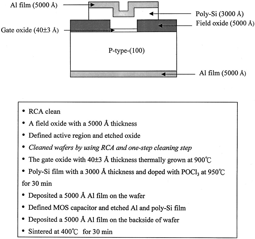
Figure 1 describes the fabrication process for capacitor and the cleaning procedure. Metal-oxide-semiconductor ~ MOS! capacitors were fabricated on a 4 in. diam, ~ 100! -oriented p-type wafers with a resistivity of 14-21 V cm. All wafers were fifirst cleaned by a standard RCA two-step cleaning method. A 5000 Å fifield oxide was thermally grown at 1050°C for 1 h in a pyrogenic gas as an isolation layer. The active region was defifined with lithography and etching. All wafers were cleaned by sulfuric acid/hydrogen peroxide mixture ~ SPM! (H2SO4 /H2O2) and diluted HF, then followed by various cleaning solutions and various methods ~ Table II! . Immediately, a gate oxide with 40 6 3 Å thickness was thermally grown at 900°C. The oxide thickness was determined from spectroscopic ellipsometry. After oxidation, a 3000 Å poly-Si fifilm was deposited at 620°C in a low-pressure chemical vapor deposition ~ LPCVD! system. The poly-Si fifilm was then doped with POCl3 at 900°C for 30 min, which resulted in a resistivity of 30-40 V /h . A 5000 Å Al fifilm was deposited on the wafer using a thermal coater. The gate of MOS capacitor was defifined by lithography, and then Al and poly-Si fifilms were etched by wet etching solutions. The back of the wafer was also deposited with 5000 Å Al fifilm using evaporation method. Finally, all the samples were sintered at 400°C for 30 min in an N2 ambient to form a good ohmic contact.

Fig1
Electrical properties for various cleaning methods.—In Fig. 7, the current density vs. electric fifield characteristic ~ J-E characteristic! of the MOS capacitor cleaned by four solutions are shown. The MOS capacitor using the ED method demonstrates the lowest leakage current density among these four samples. On the other hand, the MOS capacitor using the TE method depicts the largest leakage current density and the lowest breakdown fifield. The variation in leakage current density and breakdown fifield strength is attributed to the rough silicon surface resulting from the TE cleaning solution. Figure 8 shows the cumulative distribution ~ in percentage! of leakage current density measured at 2 3.3 V. It is clear that the ED method has the lowest distribution among these four solutions, and TE method exhibits the highest leakage current density distribution. The breakdown fifield is shown in Fig. 9. It is obvious that the TE method exhibits the lowest breakdown electric fifield in the distribution.
上一篇: 晶圆清洗:湿法仍然领先
下一篇: 硅的低温表面清洗及其在硅MBE中的应用