Some important factors that affect the dimensional control of oxide films on silicon were studied. Both Nand P -type silicon with resistivities in the range of 0.014 to 200 ohm -cm and a (111) surface orientation were employed in this experiment. The etching rates of silicon dioxide in hydrofluoric acid (IIF) were studied as a function of the concentration of HF, temperature, and stirring speed. The experimental results show that the etching rates varied directly with these variables, but no difference in etching rate was found due to concentration or type of impurity in the silicon substrate over the range studied.
The oxide layers on silicon used in this experiment were prepared by five different oxidation methods. They are: wet oxygen, dry oxygen, steam, wet nitrogen during diffusion of boron, and dry oxygen during diffusion of phosphorus. The etching rates of the oxide layer grown by the above methods have the same average value except for the oxide layer grown in dry oxygen during a phosphorus diffusion which has a much faster etching rate.
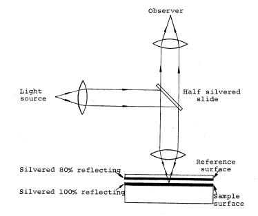
The thickness of the oxide layers employed in this experiment was determined by a multiple -beam interference method. Comparisons of this method to other optical interference methods were made. It was found that the multiple -beam method was the most accurate of the four interference techniques.
The oxide film on a silicon surface has the property of masking against certain elements from diffusing into the silicon. Therefore, it is widely employed in the fabrication of semiconductor devices. With the development of integrated circuits, the precise geometric control of the mask is becoming more important. The dimensional control of the oxide film involves how the oxide film is grown, and the method of sectioning.
In order to understand the important factors that affect the dimensional control of chemical etching, it is necessary to investigate the important variables involved and their effects on the kinetics of the etching rate of the silicon dioxide layer. The results of this study are concerned with how the concentration of the etchant, the temperature, and the stirring speed affect the etching rate. Also comparisons were made on the etching rates of silicon dioxide layers which were prepared in different thermal oxidation atmospheres. These are: wet oxygen, dry oxygen, steam, wet nitrogen during a boron diffusion, and dry oxygen during a phosphorus diffusion. These studies are designed to clarify some of the surface problems that are associated with semiconductor device fabrication.
Both N -and P-type silicon with resistivities in the range of 0.014 to 200 ohm -cm were cut into circular slices about 10 mm in diameter, 0.60 mm in thickness, and in (111) surface orientation. These samples were mechanically lapped with 600 grit silicon carbide on a Beuhler polishing machine, and then polished to a mirror finish with 1 micron alumina powder as a final abrasive. Then they were degreased in hot acetone and rinsed first in 48% hydrofluoric acid and then in deionized water. Some of the samples were further chemically polished in a solution consisting of 10 parts of concentrated nitric acid to 1 part of 48% hydrofluoric acid to 6 parts of glacial acetic acid. Thermally grown layers were prepared on the mechanically polished samples as well as the chemically polished samples.

Fig1
For the thickness of the oxide films in the range of about 2000 to 12,000 Á, the 95% confidence interval for these four methods was evaluated from a set of six samples by taking five readings from each sample for each method. The 95% confidence intervals of the standard deviation of a normal distribution (2, p. 225) were 148<o<222 for the two -beam interference method with metallized samples, 210<0<357 for the two -beam interference method with non -metallized samples, 171« <296 for the wedge method, and 71<a<126 for the multiple - beam method. Hence, the conclusion was drawn that the multiple -beam method is most accurate, and therefore, this method was employed in the present experiment.
The etching was carried out in a specially constructed apparatus which provided a close control of the etchant temperature as well as a means for stirring the solution at a constant rate. The etching solution was contained in a 100 milliliter plastic beaker which was held by clamps connected to a motor. Most of the beaker was immersed in a tank of water which was kept at constant temperature. Figure 6 shows a schematic of the apparatus.
The mechanically polished and chemically polished silicon wafers- 'were= oxidized in, wet oxygen, then etched together in 12% HF at a temperature of 25 °C and at a stirring rate of 100 rpm. The experimental results indicated no detectable difference in etching rates for the two types of surfaces.
上一篇: 过氧化氢:可持续发展的关键化学品
下一篇: 金刚石集成光机电路