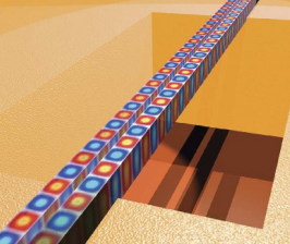
Diamond offers unique material advantages for the realization of micro- and nanomechanical resonators because of its high Young’s modulus, compatibility with harsh environments and superior thermal properties. At the same time, the wide electronic bandgap of 5.45 eV makes diamond a suitable material for integrated optics because of broadband transparency and the absence of free-carrier absorption commonly encountered in silicon photonics. Here we take advantage of both to engineer full-scale optomechanical circuits in diamond thin fifilms. We show that polycrystalline diamond fifilms fabricated by chemical vapour deposition provide a convenient wafer-scale substrate for the realization of high-quality nanophotonic devices. Using free-standing nanomechanical resonators embedded in on-chip Mach–Zehnder interferometers, we demonstrate effificient optomechanical transduction via gradient optical forces. Fabricated diamond resonators reproducibly show high mechanical quality factors up to 11,200. Our low cost, wideband, carrier-free photonic circuits hold promise for all-optical sensing and optomechanical signal processing at ultra-high frequencies.
In this work, these limitations are overcome by direct overgrowth of wafer-scale substrates with diameters up to 6 inch. We employ high-quality silicon substrates, which provide an atomically flflat surface. A low-refractive index buffer layer is grown by thermally oxidizing the wafer to a thickness of 2 mm. During the oxidation process, the surface morphology is preserved, providing a smooth starting layer for the later diamond growth. Microcrystalline diamond layers are then deposited directly onto the oxidized substrates. To initiate the later growth of diamond on our substrates, fifirst, a diamond nanoparticle seed layer is deposited onto the SiO2 fifilm by ultrasonifification for 30 min in a water-based suspension of ultra-dispersed (0.1 wt %) nano-diamond particles of typically 5–10 nm size30. Then samples are rinsed with de-ionized water and methanol. After dry blowing, the wafer is transferred into an ellipsoidal 915 MHz microwave plasma reactor31, where diamond fifilms with a thickness below 1 mm are grown at 1.8 kW microwave power, using 2% CH4 in 98% H2, at a pressure of 80 mbar and a temperature of 850 ℃. Substrate rotation was applied to avoid angular non-uniformities arising from the gas flflow. Growth rates were in the range of 1–2 mm h1. After growth, the samples are cleaned in concentrated HNO3:H2SO4 to remove surface contaminations.
Diamond nanophotonic circuits are then realized using a combination of electron-beam (e-beam) lithography and pattern transfer into the thin fifilm via reactive ion etching (RIE). We employ the negative e-beam resist Fox15, which enables resist thickness of several 100 nm. Upon exposure, Fox15 provides an anorganic glass-like protection layer, which is resistant to oxygen plasma in contrast to organic e-beam resists. High-resolution photonic circuits are written using a JEOL 5300 50 kV e-beam system. After developing, the negative tone images are transferred into the diamond layer using reactive ion etching in an Oxford 80 Plasmalab etcher in oxygen-argon (O2/Ar) chemistry. The etching step is carefully controlled by timing in order to obtain a desired target depth within the diamond substrate.

Fig1
Our integrated optical components are realized starting with commercial silicon wafers, single-sided polished. The substrates are thermally oxidized to a target oxide thickness of 2 mm. The oxide thickness is optimized in order to provide best coupling effificiency with our grating coupler design. Microcrystalline diamond is then deposited with a thickness of 600 nm by plasma enhanced CVD. Ridge waveguides are fabricated using a combination of electron-beam lithography and reactive ion etching. In order to provide high etching selectivity, we employ Fox15 electron-beam photoresist, which is deposited with a thickness of 500 nm on the diamond thin fifilm. A timed reactive ion etching process is then performed in oxygen/argon chemistry, with a typical etch rate of 25 nm min. For the optimal coupling effificiency, the diamond thin fifilm is etched down to a residual thickness of 300 nm. For the fabrication of free-standing structures, a second lithography step is used to defifine opening windows for subsequent wet etching. We employ chromium as the masking material against the RIE plasma. The chromium layer is structured using a PMMA positive resist mask. Afterwards the chromium layer in the exposed areas is removed using chromium etchant solution (Sigma-Aldrich Chromium Etchant 651826) and the PMMA is subsequently removed in acetone and ashing in oxygen plasma. After the second RIE step, the underlying oxide layer is isotropically etched in buffered oxide etchant (6%) and subsequently in chromium etchant to remove the remaining chromium layer throughout the wafer. Finally, the fifinished samples are transferred to methanol and rapidly dried on a hot plate.
上一篇: 二氧化硅薄膜的化学蚀刻
下一篇: 二氧化碳低温预处理后湿清洗去除光刻离子胶