In FEOL processing, doping of active areas like source, drain, and extensions (NMOS and PMOS) is done by ion implantation. Un-doped regions are covered with photoresist to protect them from implantation. Ion implantation modifies the surface of the photoresist to generate a dehydrogenated amorphous carbon layer, the crust . When the implant conditions are more aggressive (higher implant energy and implant dose), the hard crust becomes more and more challenging to be removed. Conventionally, a plasma ashing process followed by a wet cleaning, typically SPM (Sulfuric acid/Hydrogen peroxide mixture) chemistry, can remove the implanted photoresist, but usually leads to damage and strong oxidation of the underlying semiconductor material and hence result in material or dopant loss. As the technology node migrates beyond 45nm, the photoresist removal process should also be compatible with novel materials such as high-k dielectric and metalgate used in advanced gate stack integration. For these reasons, it is desirable to eliminate the plasma ash and SPM clean chemistry. Wet only PR removal process is studied using new chemistries like solvents that are compatible with the other FEOL process steps, however, the photoresist removal using solvents only still showed lower removal efficiency than conventional processes. It has been demonstrated that the CO2 cryogenic pre-treatment can improve the ion implanted photoresist stripping efficiency of the wet cleaning processes, and can also enhance the photoresist removal efficiency by the solvents.
In this paper, the impact of the CO2 cryogenic pre-treatment on the stripping of ion implanted photoresist was studied in both SPM-based and solvent-based cleaning chemistries processes without plasma ashing.
The CO2 cryogenic pre-treatment has been performed on the WaferClean™ 3600 (WC3600), a 200- 300 mm wafer bridge tool from Eco-Snow Systems. CO2 cryogenic aerosol cleaning process has been already studied for removal of particles and stripping of photoresist . The CO2 cryogenic treatment uses liquid CO2 at 58.6 bar (850 psi) and 25°C, expanding through a specially designed nozzle. The expansion of liquid CO2 through the nozzle creates solid and gaseous CO2 in a highly directional and focused stream. During the CO2 treatment, the entire surface of the wafer is scanned with a broad spray nozzle assembly that is larger than the wafer diameter. Highly purified liquid CO2 (PrecisionClean CO2 from Eco-Snow Systems) stored in aluminum cylinder is used as CO2 source for the WC3600 system to keep the hydrocarbon at the ultra-low contamination levels that are required by the microelectronic manufacturing. The CO2 aerosol treatment is aimed at breaking the photoresist crusted top layer, and subsequently improving the stripping efficiency of the wet chemical cleaning.
The CO2 cryogenic process parameters were optimized to maximize the photoresist removal efficiency during the wet stripping process and to minimize the damage on FEOL structures. Damage analysis was performed by KLA-Tencor 2800 patterned wafer inspection system for the cryogenic CO2 spray condition used for implanted photoresist removal. Poly-silicon line structures (meander-fork) with line width down to 70 nm are used for damage evaluation. Defect analysis on damage vs feature line width is on going.

Fig1
It is clearly demonstrated that faster photoresist removal and higher efficiency are obtained when the wet clean is combined with a CO2 pre-treatment. Removal efficiency increases as the ion implanted energy is decreasing. SPM shows higher removal efficiency than solvents, but solvent clean is needed for advanced device. Within all solvents screened, NMP and DMSO showed the higher removal efficiency, and CO2 treatment enhances the removal efficiency of all solvents tested. High removal efficiency of ion implanted photoresist on 300 mm wafer is observed by optical microscopy when cleaned with NMP in single wafer tool after CO2 pre-treatment. Evaluation of the removal efficiency is continuing on patterned poly-silicon wafers.
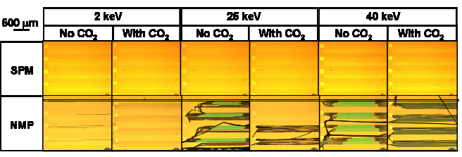
The ion implanted photoresist removal efficiency has been evaluated after CO2 pre-treatment on full 300 mm wafers. 248 nm DUV photoresist is implanted with As ions at 3x10 15 atoms/cm2 for 3 different energies (2 keV, 25 keV and 40 keV). SU3000 single wafer tool from DNS with NMP nanospray has been employed for wet clean. Visual and optical microscope inspection shows that without cryogenic CO2 pre-treatment, most of the photoresist remains on the wafer after NMP clean while only residues on fine structures are visible on 25 keV and 40 keV wafers processed with cryogenic CO2 pre-treatment. Further inspections (KLA-Tencor 2800, top down SEM review on polysilicon structures) are ongoing to better quantify the PR removal efficiency with and without CO2 pre-treatment. Figure 4 shows comparison with and without CO2 treatment on 25 keV implanted wafers.
上一篇: 金刚石集成光机电路