Photolithography is the preferred method of micro-patterning, not only in electronics manufacturing but also in such emerging areas as micro-electromechanical systems (MEMS), micro-fluidics and ‘digital optical chemistry. The process normally requires a customproduced hard photo-mask to be manufactured, which is expensive, time consuming, and often limits flexibility. Much research has therefore gone into developing mask-less photolithographic methods for rapid prototyping,laser direct writing which is now a commercial technique. Other mask-less approaches also under development include projection writing using a single spatially filtered light emitting diode (LED), and various spatial light modulator (SLM) and digital light projector (DLP) based methods.
Micro-pixelated gallium nitride LED’s (‘micro-LEDs’), consisting of arrays of individually addressable micrometer-sized light emitting pixels, are being investigated by several groups for applications in areas including micro-displays, bioscience and instrumentation. These devices offer spatio-temporal control of the emission pattern, and also spectrally selective excitation because the emission bandwidth is typically narrow (~15nm full-width at half maximum (FWHM)), with the central wavelength being defined by the semiconductor epitaxy of the light-emitting quantum wells. Indeed, in a preliminary demonstration we were able to show some simple micrometer-sized exposure patterns in photoresist achieved by a ‘first generation’ array designed to operate at an approximately iline photolithography wavelength (365nm). More recently, the technology has advanced to the point where much higher powers are available per pixel through flip-chip bonding of the devices and independent element addressing by custom CMOS control circuitry is possible.
Here we explore the implications for mask-free photolithography and other forms of optical direct-write patterning engendered by these recent developments. A CMOS-controlled 8 x 8 flip-chip 370nm gallium nitride-based micro-LED array demonstrator is de-magnified through various combinations of back-to-back microscope objectives. The CMOS is shown to be capable not only of controlling the emission pattern, but also the exposure dose. We show example structures written in positive as well as in negative photoresist. The system can be used to directly reproduce the pattern on the micro-LED array and/or lines can be written by moving the sample while one or several LED pixels are turned on. Our system can be considered to bridge the gap between low cost, but low resolution, mask-less prototyping techniques, such as the use of a photocopier , toner mediated lithography, or etching through a mask made using a cutter plotter (feature size limited to over 200µm) and high cost methods competing with traditional optical projection lithography (OPL) in terms of resolution, such as scanning electron-beam lithography (SEBL), focused ion-beam (FIB) lithography, interference lithography (IL), maskless optical-projection lithography (MOPL), and zone-plate-array lithography (ZPAL).

Fig1
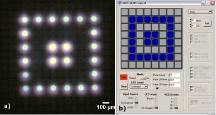
The CMOS control device was attached to a printed circuit board (PCB), which is computer controlled via a field programmable gate array (FPGA) board (XEM3010-1000 from Opal Kelly). In the custom-made software interface, shown in Fig. 1(b), the mode of operation of the CMOS chip can be set to linear feedback shift register (LFSR, not used in this work), DC/External (if no external clock is present this is CW operation), or VCO. The LED mode can be set to either DC/Square (CW operation or a square wave clocked to the external or VCO frequency) or Pulse (pulse at a controllable duration with the repetition rate set by external or VCO frequency). The VCO divider sets a value (1, 4, 16, or 64) with which the VCO frequency is divided before it is used. A pixel or a pattern consisting of a set of pixels can be chosen either by setting the row and column [upper right corner in Fig. 1 (b)] or by highlighting the desired pixels in the grid pattern of the software interface. With the timing control the LED on-time can be set accurately down to ~100ms.
A photographic image and a corresponding schematic of the setup for mask-less photolithography can be seen in Fig. 2. The setup consists of the CMOS driven computer controlled micro-LED device mounted vertically on a manual XYZ stage, a horizontallymounted infinity-corrected microscope objective (Nikon CFI Plan Fluor Series) for light collection (collection objective), a mirror to direct the light downwards, a 50-50 UV beamsplitter cube, and a second (vertical) infinity-corrected microscope objective (projection objective), mounted on a Z-translation stage, to project the LED array image onto the sample. A CCD camera (Prosilica EC650C) with zoom lens attachment (Navitar, 11-110mm) adjusted to focus at infinity is used to monitor the position of the sample or the LED array depending on the orientation of the beam-splitter. Infinity-corrected objectives give collimated (or parallel) output beams of the object in the focal plane, hence when the camera objective is set to focus at infinity, the image displayed on the camera is optically conjugate to the focal plane of each objective.
上一篇: 硅与玻璃晶圆键合的键合能研究
下一篇: 基于硅的多芯片LED封装