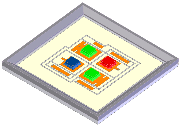
Light emitting diodes (LEDs) not only significantly reduce power consumption compared to incandescence, but also with longer lifetime, fast response speed, compact size, low maintenance cost and grater reliability. Therefore, they have gained widespread use since their inception in the early 60’s. Moreover, special deposition techniques have made possible LEDs with much higher brightness than traditional devices. This opens up many new applications such as backlighting for displays, automotive lighting and new consumer products like flash for mobile camera or compact projects .
Nevertheless these possibilities, there are some remain problems like optical efficiency, thermal resistance, cost and brightness to completely substitute the conventional solidstate lighting like a fluorescent light, incandescent lights. Many researches are progressed to ameliorate the problems stated above in various fields. But most of the previous researchers on high brightness LEDs have focused on how to improve the chip characteristics. Few of them discussed the package point of view. Among them, optical efficiency, multi chip package issue and cost are the representative problems to be improved before everything for commercializing. In LEDs, silicon based multi chip package is produced to overcome the problems related to the optical efficiency, thermal resistance, multi chip package issue and cost using lead frame type conventional package. However the conventional packages like lead frame type have the limitation of accuracy, cost, thermal resistance and expansion to the multi chip packaging. Through suggested silicon based multi chip LED packaging, wafer level fabrication & packaging technology is realized. It can not only solve problems of conventional packaging structures but also tremendously improve the optical properties of LED packaging like optical efficiency, reduce the manufacturing cost of LED package using WLP (wafer level packaging) and increase the expansion possibility module package using silicon based platform.
In many research fields, MEMS (Micro Electro Mechanical System) technology is used to accomplish silicon based LED PKG structure which can be applied wafer level fabrication and packaging. However the existing LED package structures have critical problem which the color mixing for white color is difficult because of its difficulty of expansion limitation for discrete lead frame type package. Multi chip package for high power LED application like solid-state lighting are required that optimized chip distance for color mixing, high performance of thermal resistance and high optical extraction efficiency. Among various fabrication methods for multi chip LED package, lead frame type package and ceramic based package are generally used. In case of lead frame type package, it has difficulty in expansion possibility for arrayed package. Additionally, it has high thermal resistance compared with another packaging technology. Ceramic based package has difficulty for expansion possibility for arrayed package because of its warpage in firing process. However, due to a lot of research in semiconductor fabrication process, silicon based LED package has many advantage like expansion possibility for arrayed package, thermal resistance, mass production, cost and so on. In this study, the new silicon based multi chip package is investigated. 9mm x 9mm with 0.65 thickness package array is fabricated and optimized chip distance is determined.

Fig1
After optical and thermal analysis, as we mentioned above, the silicon based multi chip LED package which has 9mm x 9mm with 0.7mm thickness is designed. This package is composed 4 chips (1 red, 2 green, and 1 blue) in 1 cavity. 2 green chips are parallel connected on top surface. Total 5 masks are used for fabrication.
Base substrate fabrication starts with a <100> silicon wafer. First step is dry etching for bottom pad, trench, and via hole using ICP equipment. Etch depth is 20um, 150um, and 280um (a, b, c). The via hole diameter is 80um. Oxide is coated on etched wafer using oxidation process. This step makes insulation layer (d). The layer of Ti/Au is sputtered for seed layer. After this deposition process, Cu is electro plating for interconnection (e). After polishing process (f), Al layer is deposited in top surface for increasing reflectivity (g). Next step is Al, Au layer patterning process. Metal layer is patterned using standard photolithography and wet-etched in Al/Au etching solution (h). The last step in base substrate process is Au/Sn patterning process. This process is performed for eutectic bonding with base substrate and reflector cup substrate.
Reflector cup process start with a <100> silicon wafer on which has a 1500 A thickness silicon nitride film. First step is anisotropic wet etching of silicon (Si) for reflector using THAH (Tetramethyl ammonium hydroxide) solution. Etch depth is 350 µm (a, b). The layer of Ti/Au is evaporated for eutectic bonding layer (c). The last step is metal deposition process for increasing reflectivity. According to this deposition process reflector which has reflectivity, over 70% at all wave length is realized. This result shows in figure 13. Finally, figure 14 shows the realized multi chip LED package.
上一篇: 无掩膜紫外光刻技术
下一篇: LED光刻技术快速制造微流控芯片