Microfluidic chips are generally fabricated by a soft lithography method employing commercial lithography equipment. These heavy machines require a critical room environment and high lamp power, and the cost remains too high for most normal laboratories. Here we present a novel microfluidics fabrication method utilizing a portable ultraviolet (UV) LED as an alternative UV source for photolithography. With this approach, we can repeat several common microchannels as do these conventional commercial exposure machines, and both the verticality of the channel sidewall and lithography resolution are proved to be acceptable. Further microfluidics applications such as mixing, blood typing and microdroplet generation are implemented to validate the practicability of the chips. This simple but innovative method decreases the cost and requirement of chip fabrication dramatically and may be more popular with ordinary laboratories.
Microfluidics is widely believed to be one of the keys to nextgeneration technology for biochemical analyses, including high-throughput protein or cell biochemical assays in laboratories or diagnostics of body fluid in clinical applications, which would reduce costs tremendously both in time consumption and amounts of chemicals due to the reduction in volume from milliliters to nanoliters or even picoliters for chemical reactions. To date, most microfluidic devices are fabricated through soft lithography derived from the fabrication of integrated circuit boards based on lithography. Thanks to Whiteside’s work, the flexible poly(dimethylsiloxane) (PDMS) was found to be a simple, low cost alternative to classical mold materials. Though people have also been devoting themselves to developing other convenient and lower-cost methods for fabrication of microchips such as waxing dipping , glass-based chips and paper-based chips , soft lithography, especially the replica molding method, is still the most popular method for rapid prototyping of microfluidic chips.
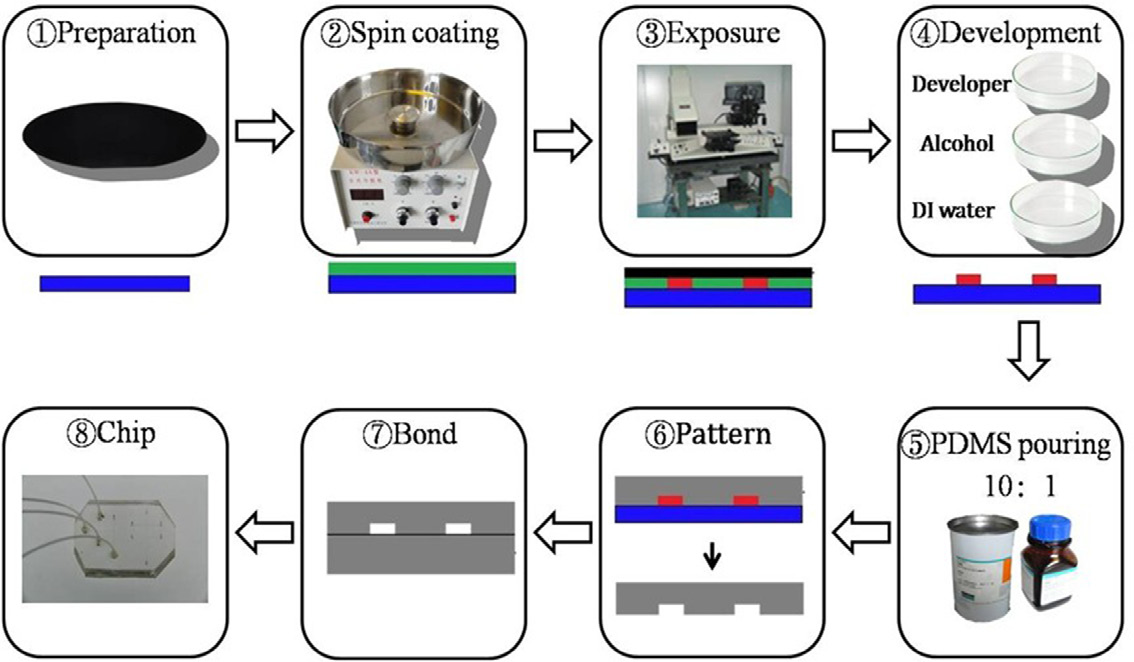
Soft lithography is a diverse set of techniques using elastomeric materials for rapid prototyping, and replica molding is one of the most common methods. In essence, replica molding refers to a procedure employed to fabricate PDMS chips against relief structures made of photoresist on a silicon wafer. There are many advantages for using PDMS for replica molding, such as low cost, fast process, non-defect replication from SU-8 master, easy sealing and bonding to other substrates, suitability for biological and cellular applications and so on. The detailed progress is shown in figure 1, and we note that the fabrication of the SU-8 patterned master involves traditional photolithography, which requires the most expensive equipment of all the steps due to the expensive machine maintenance and high environment requirement.

Fig1
Soft lithography is a diverse set of techniques using elastomeric materials for rapid prototyping, and replica molding is one of the most common methods. In essence, replica molding refers to a procedure employed to fabricate PDMS chips against relief structures made of photoresist on a silicon wafer. There are many advantages for using PDMS for replica molding, such as low cost, fast process, non-defect replication from SU-8 master, easy sealing and bonding to other substrates, suitability for biological and cellular applications and so on. The detailed progress is shown in figure 1, and we note that the fabrication of the SU-8 patterned master involves traditional photolithography, which requires the most expensive equipment of all the steps due to the expensive machine maintenance and high environment requirement.
The photomasks with the desired patterns are designed in CorelDRAW software and then printed on high-transparency photographic sheets. Before exposure, the mask is placed directly on the photoresist and the lamp is vertically fixed on the support. According to the scale, we can adjust the height between the support and platform to control the separation distance between the light source and the substrate. When the distance is set to be 1cm, Si wafers with a layer (40µm) of SU-8- 2050 photoresist are exposed through the mask for 3min to form a channel with the widths of 10–400µm and height of 40µm. Repeating the well reported patterns made by technical exposure machines, this portable LED UV light source really reduces both the complexity in the operation procedure and the requirement of conditions for fabricating microfluidics chips in laboratories.
上一篇: 基于硅的多芯片LED封装
下一篇: 晶圆级芯片级封装的背面保护