Atomic layer etching (ALE) typically divides the etching process into two self-limited reactions. One reaction passivates a single layer of material while the second preferentially removes the passivated layer. As such, under ideal conditions the wafer scale uniformity of ALE should be independent of the uniformity of the reactant fluxes onto the wafers, provided all surface reactions are saturated. The passivation and etch steps should individually asymptotically saturate after a characteristic fluence of reactants has been delivered to each site. In this paper, results from a computational investigation are discussed regarding the uniformity of ALE of Si in Cl2 containing inductively coupled plasmas when the reactant fluxes are both non-uniform and non-ideal. In the parameter space investigated for inductively coupled plasmas, the local etch rate for continuous processing was proportional to the ion flux. When operated with saturated conditions (that is, both ALE steps are allowed to selfterminate), the ALE process is less sensitive to non-uniformities in the incoming ion flux than continuous etching. Operating ALE in a sub-saturation regime resulted in less uniform etching. It was also found that ALE processing with saturated steps requires a larger total ion fluence than continuous etching to achieve the same etch depth. This condition may result in increased resist erosion and/or damage to stopping layers using ALE. While these results demonstrate that ALE provides increased etch depth uniformity, they do not show an improved critical dimension uniformity in all cases. These possible limitations to ALE processing, as well as increased processing time, will be part of the process optimization that includes the benefits of atomic resolution and improved uniformity.
Plasma based ALE is a self-limiting two-step process capable of removing single atomic layers in each cycle. The first step of the cycle passivates the surface in a manner that naturally stops when the top surface layer is fully passivated. This step is ideally performed with an ion-free flux of neutral radicals. In the second step, the passivated layer is selectively removed by, ideally, a radical free flux of energycontrolled ions that chemically sputters the top passivated layer but is not energetic enough to sputter the underlying unpassivated atoms. When the fluence of reactants is large enough to fully saturate both of the self-limited half-reactions, the etch depth per cycle (EPC) should be constant. In this saturated regime, the etch rate should also be independent of small non-uniformities in the reactant fluxes. The adoption of ALE techniques may then offer a way to obtain atomic scale uniformity over large areas without the need for having correspondingly uniform reactant fluxes.
Self-limiting behavior is necessary to improve wafer scale uniformity in the presence of non-uniform reactant fluxes, but it is not clear what the relationship is between the uniformity enabled by ALE and process saturation. Most ALE processes are not perfectly self-limited , and it is difficult to estimate the effect of non-ideal etching reactions on process uniformity. The following discussion focuses on the consequences of saturation during the ion bombardment phase of ALE on wafer-scale uniformity, however the same trends hold true for the passivation phase as well.

Fig1
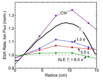
ALE using an ion bombardment time of 3 s produced significantly more uniform etch rates than continuous etching, with only a small positive correlation between etch rate and ion flux, as shown in figure 2(b). For antenna A1, the etch rate—measured here in monolayers of computational cells (3 Å) per cycle—increased by 17% from the center of the wafer to the edge, significantly less than the increase in Γi (133%). This improvement in etch uniformity compared to Γi indicates a fully saturated self-limited ALE reaction. Non-ideal continuous etching mechanisms result in some dependence of etch rate on Γi, and produce the remaining non-uniformity in etch rate.
While the ALE process significantly improved the etch rate uniformity for antenna A1 and A2 when compared to continuous etching, the results for antenna A3 are less improved. This result indicates that the ion fluence at the center of the wafer, which is similar for each antenna, is only just large enough to saturate the ion bombardment reaction. For the A1 and A2 antennas, the ion flux and fluence increase with radius. Given that both the passivation and ion phases are both fully saturated, the increasing fluence at larger radius does not produce a significantly higher etch rate. However, in the case of antenna A3, the ion fluence drops below saturation as the radius increases, causing the etch rate to depend more strongly on ion flux which decreases with radius.
The ICP power used for antenna A3 was chosen to result in similar ion flux at the center of the wafer as antennas A1 and A2. This choice of ion flux resulted in sub-saturation behavior at large radius where ion fluxes are the lowest when processed using the same ion bombardment time as A1 and A2. If the ion fluence was increased for case A3 so that the entire wafer was within the saturation regime, either by increasing the ICP power (resulting in a larger ion flux) or by increasing Ti, a similar increase in uniformity could be obtained for A3.
上一篇: 用于 MEMS 的干式硅蚀刻
下一篇: 硅等离子蚀刻工艺产生的表面粗糙度