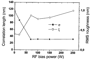
The authors used atomic force microscopy to analyze the roughness generated on c-Si (100) surfaces when etched in high-density plasmas over a wide range of conditions pressure, rf power using SF6, CF4, Cl2, and HBr chemistries. The authors demonstrate unambiguously that high-density plasmas do not generate roughness during silicon etching; but on the contrary, they tend to smooth the existing surface roughness if already present. This is evidenced by analyzing the time evolution of the shape of self-organized silicon nanopillars (patterned on the Si wafer by using diblock copolymers as an etch mask) . The 20-nm-high, 20-nm-wide pillars separated by 10 nm are rapidly smoothed by exposure to Cl2 and SF6 plasmas, thus restoring a flflat silicon surface. In high-density plasmas, the local etch rate is generally limited by the availability of reactive radicals. In these conditions, the smoothing mechanism is due to the fact that the hills of a rough surface receive a higher flflux of etchant radicals than the valleys. Finally, the authors show that the roughening of silicon surfaces in F-based plasma, often reported in the literature, is only due to the micromasking of silicon by AlFx particles originating from the sputtering of the (Al2O3) reactor walls. A high percentage of Al is indeed detected on the surface after etching in F-based plasmas. However, when the chamber walls are intentionally coated by a carbon layer prior to the silicon etching process, the F-based plasmas behave like the other etching chemistries investigated: they rapidly smooth any existing roughness.
The roughness generated in thin fifilms during their etching by plasma processes can be a serious issue for the correct operation of the fabricated device. For Si etching, this is true for integrated circuit (IC) fabrication, micro-optics, microsensors, or more generally microelectromechanical system (MEMS) fabrication.
Finally, besides studies of silicon etching in F-based plasmas, Thomas et al.studied the reactive-ion etching of silicon by Cl2 plasmas by using ellipsometry and scanning electron microscopy. They reported that plasma conditions can be found where the silicon is etched without roughness generation, or that existing roughness can even be smoothed.
Therefore, it is diffificult to conclude under which conditions that plasma etching processes are generating roughness, and what are the physicochemical mechanisms leading to the roughness formation and evolution. In this article, we used AFM to investigate systematically the roughening (or smoothing) of the crystalline silicon etch front in highdensity inductively coupled plasma. Several chemistries and operating conditions were investigated by using SF6, CF4, HBr, Cl2, and Ar. Furthermore, the chemical nature of the etched surface was investigated by total reflflection x-ray flfluorescence (TXRF) . As a result, we show that plasma etching in itself does not generate roughness; on the contrary, it tends to smooth any existing roughness. The roughness growth reported in the literature is probably due to the redeposition of nonvolatile AlF particles on the silicon wafers.

Fig1
The authors acknowledge the support of the European Commission for the project PULLNANO under Contract No. IST-026828 from the Information Society Technologies (IST) within the European Union’s Sixth RTD Framework Programme. The authors also would like to acknowledge K. Assous, M. Kogelschatz, and T. Baron for preparing the selforganized silicon nanopillar samples, and N. Sadeghi and M. Touzeau for helpful discussions.
下一篇: 硅谐振器的晶圆级封装技术