Recently, a family of low frequency silicon resonators with AlN piezoelectric activation has been developed. These devices need to be operated under vacuum. The main motivation for the packaging of resonator under vacuum is to increase the Q factor, and to guarantee the long-term stability of the resonance frequency. In order to minimize the size of packaged resonators, wafer level packaging (WLP) has been chosen.
Electronic devices of all kinds need timing references. Currently, the main technology for clock products is quartz. Miniaturization of quartz has been driven by the mobile phone industry. Today 32kHz quartz resonator are found in packages as small as 2x1.25x0.6mm3 (Epson Toyocom FC-12M) while 30MHz or above resonators can be found in 1.6x1.25x0.3mm3 packages (TEW Tokyo DenpaTAS1612C/D). Since the early 1980s, companies have been trying to replace quartz with silicon MEMS-based oscillators. Until recently however, the low temperature stability of silicon and the need for expensive ceramic or metal vacuum packaging prevented MEMS from becoming a serious alternative to quartz. SiTime claims the smallest integrated silicon resonator with electrostatic actuation packaged at the wafer level. The resonator cavity is sealed at high temperature (1000°C) and under high vacuum during the processing of the resonator itself (not a backend post-processing) . An alternative – piezoelectric through AlN - actuation solution has been proposed in recent years. Devices covering a large frequency range from 20kHz to 36MHz were demonstrated. One of the major advantages of piezoelectric devices over electrostatic devices is that the impedance levels are much closer to those achievable with quartz and would hence allow similar drive circuits to be used.
The solution uses a capping Pyrex wafer sealed by anodic bonding. This bonding method requires an extremely smooth and residue free surface of the wafer. The thickness of silicon oxide on rear side of the wafer shall not exceed 500 nm. The bonding process is conducted at 350°C, -1200V, 3 mbar during 30 min. The performances of resonators were not altered during this sealing process. Thin (300 microns) Pyrex substrates have been hermetically bonded with device SOI wafers (thickness 100+390 microns).
A reflow process was developed minimizing the size and amount of voids (thought to be Kirkendall voids), controlling the dendrite height and the amount of eutectic formed. The reflow process developed involves oxide reduction, annealing and AuSn (80/20) eutectic formation steps. A tacking process is involved before the vacuum sealing process to use the advantage of accurate alignment possible in a flipchip machine. Tacking is done using a tacking media which can be evaporated and degassed before the vacuum sealing step. The vacuum sealing is done at a peak temperature of 320ºC and the process time is optimized to have less consumption of the UBM. Pressure is needed during the sealing process to have uniform wetting throughout the ring due to the high surface tension of the AuSn eutectic. Fig.4b shows a cross section view after sealing process (UBM/Au/AuSn/UBM). In this version, the electrical contact with the resonator is established via metal lines crossing the sealing ring (Fig4c). The electrical signal and metal sealing ring are isolated by a passivation SiON layer.

Fig3
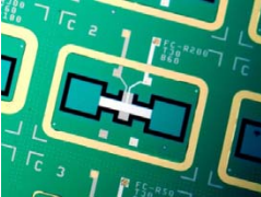
All types of resonators are built from (100)-oriented Silicon on Insulator substrates. the vibrating structure consists mainly of single crystal silicon that is oxidized on both sides (top and buried oxide), and that is topped by AlN and its electrodes. Polycrystalline piezoelectric (002) AlN films are deposited by magnetron sputtering on Pt (111) forming a piezoelectric activation for the SOI structure. All thin films are patterned by standard photolithography and dry etching. The Si beams are created by deep reactive ion etching (DRIE) of the Si device layer from the top side, followed by the DRIE of the Si handle from the backside. Fig.3 shows a top view of 1MHz extensional and 100kHz flexural AlN/Si resonators with sealing rings.
上一篇: 硅等离子蚀刻工艺产生的表面粗糙度
下一篇: SC-1处理后的硅晶片的TXRF分析