Silicon wafer cleaning is the most frequently applied processing step in the integrated circuit manufacturing sequence. This process is intended to remove several different types of contaminants, among them particles, metallics, and organics. It has been estimated, however, that over fifty percent of yield losses in integrated circuit manufacturing are caused by contamination remaining on the surface of silicon wafers after cleaning. It is the object of this article to document the effects of using improved, ultrahigh purity chemicals on silicon wafer surfaces as measured by total reflection x-ray fluorescence, TXRF. During this study, silicon samples were cleaned with standard grade chemicals and ultrahigh purity chemicals, and metallic impurities were then measured with TXRF. It was found that the use of ultrahigh purity chemicals substantially reduced the amount of surface contamination present on wafer surfaces after cleaning.
Silicon wafer cleaning has remained an integral part of semiconductor device fabrication since the 1950s, and in fact, is the most frequently applied processing step in the integrated circuit (IC) manufacturing sequence.The objective of wafer cleaning is the removal of contamination from the silicon surface without degrading its texture. The importance of adequate cleaning cannot be underestimated in that contamination remaining on the substrate surface is known to degrade device performance, reliability, and yield. It has been estimated that over fifty percent of yield losses in IC manufacturing are caused by microcontamination.Wafer cleaning will continue to remain an important process step in device manufacturing especially as device geometries approach sub-half micron dimensions.
Contamination remaining on a semiconductor surface can cause a variety of adverse effects during subsequent processing that will depend on the nature of the impurity. Particles can cause blocking or masking of various processing operations, for example during etching or photolithography. Particles present during film growth or deposition can lead to pinholes and microvoids, and if sufficiently large and conductive, will cause shorting between conductor lines. Metallic impurities will also contaminate the silicon wafer surface at almost any step in device processing. Such contamination will contribute to the increase of current leakage at the p-n junction, decrease of oxide breakdown voltage, and deterioration of minority carrier lifetime.Many metals are capable of introducing localized energy states close to the middle of the silicon bandgap (1.12 eV), thereby creating efficient generation-recombination centers that degrade minority carrier lifetime. These centers are otherwise known as traps. For example, by introducing bulk traps at 0.40 and 0.55 eV above the silicon valence bandedge, iron may cause leakage currents that prevent dynamic random access memory (DRAM) devices from meeting refresh specifications.
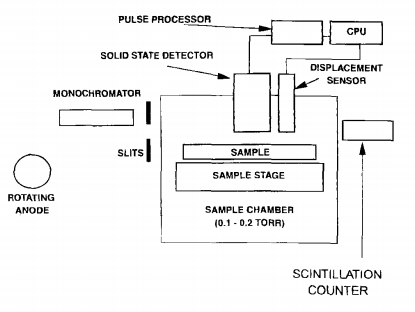
In TXRF, monochromatic x-rays impinge on an optically flat sample surface at an angle below the angle for total external reflection and excite only the top few atomic layers (about 3-8 nm in depth). The fluorescence x-rays from these top few monolayers emit in many directions, and a detector located perpendicular and close to the sample surface collects the emitted fluorescence x-rays and analyzes them according to energy. It is this energy analysis which yields elemental identification.

Fig1
During the study; chemicals (H202 and NH4OH) were supplied to the Silicon Products Department in Sherman by the Chemical Operations Department in Dallas. Initially, the materials were of the standard grade but were later switched to ultrahigh purity. Specifications (highest acceptable tolerances of an impurity) for the four metals that were tracked during the study (Zn, Cu, Ni, and Fe) are listed in Table I. As can be seen, the switch to the higher purity grade chemicals resulted in tolerances that are tighter by 30-100 times.
There is a definite correlation between impurity levels in process chemicals and metal deposition on wafer surfaces. It was further shown in this study that TXRF is an appropriate tool for the detection and measurement of surface wafer impurities.
上一篇: 硅谐振器的晶圆级封装技术