This paper discusses surface texturization of monocrystalline silicon wafer h100i by using a very simple and cost effective technique consisting of a combination of mechanical grinding and chemical etching, to achieve desired surface reflflectance for solar cell applications. The abrasive used for mechanical grinding is aluminum oxide powder with different grain sizes. Potassium hydroxide– isopropyl alcohol solution (with different molar concentrations) is used as alkaline etchant. The change in surface reflflectance may be correlated with the change in surface roughness parameters of silicon wafer after texturing. The roughness measurements are performed by using white light interferometry based three dimensional optical pro- fifiler. Reflflectance measurements of texturized silicon wafer samples are carried out by ultra violet visible spectrophotometer. A comparative reflflectance study of silicon wafer samples after using these methods reveals that the combination of mechanical grinding and alkaline etching is more effective for surface texture modifification in terms of signifificantly reduced surface reflflectance as compared to a single texturization technique. After reflflectance data analysis of texturized samples, correlations have been established for percentage reflflectance versus abrasive grain size and percentage reflflectance versus molar concentration of etchant. These correlations provide a combination of abrasive grain size and etchant molar concentration to achieve desired value of percentage surface reflflectance of silicon wafer from 23.97 to 11.85% at 800 nm wavelength, which is signifificant for solar cell applications.
These pyramidal structures are distributed randomly on silicon wafer surface and are known as random pyramids. They cause effective light trapping inside silicon, thus enhancing the effificiency of solar cell. For silicon solar cells, visible light with a spectral range of 400–800 nm is the most energetically-dense part for conversion into electricity, thus the present study is conducted with a focus on spectral range 400–800 nm.
Other advance techniques for surface texturing such as electrochemical passivation, laser texturing and surface coatings used by many researches, claim to show better results than mechanical grinding and alkaline etching, but most of them are complex and costly. The present state-of-the-art for surface reflflection of silicon wafer in photovoltaic industry is around 3–4%, but these results require complex experimental procedures and costly instruments. In this study we propose a simple and cost effective technique by combining mechanical grinding and chemical etching, for reflflectance reduction and report detailed analysis of textured silicon wafer surface parameters.

Fig5
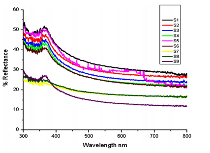
Analysis of reflflectance results of silicon wafer samples texturized by using mechanical grinding reveals that the reflflectance over the range of wavelengths studied is also lowered as a result of grinding only. A considerable change in reflflectance is observed with change in the grain size of Al2O3 powder (from 8 to 22 lm). The lowering of reflflectance may be attributed to increase in average surface roughness parameters Ra and Sa and total surface roughness Rt.
By solving these quadratic equations we can provide a combination of abrasive grain size and etchant molar concentration to achieve any value of percentage reflflectance from 11.85 to 23.97% at 800 nm wavelength. Figure 5 shows a plot between percentage reflflectance, abrasive grain size and etchant molar concentration for those samples which are texturized by using a combination of mechanical grinding and chemical etching.
Surface morphology of some samples shows sharp structures on silicon wafer surface. The reduced surface reflflectance of these samples as compared to the polished silicon wafer may be attributed to the structures formed on wafer surface after texturing and may be correlated with increase in roughness.
上一篇: SC-1处理后的硅晶片的TXRF分析