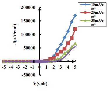
In this work, the nanocrystalline porous silicon (PS) films is prepared by photoelectrochemical etching of n-type silicon wafer with different currents density (20, 35 and 50 mA/cm2 ) and etching time 15 min on the formation nano-sized pore array with a dimension of around few hundreds nanometric. The films were characterized by the measurement of FTIR spectroscopy and atomic force microscopy properties.Chemical fictionalization during the photoelectrochemical etching show on surface chemical composition of PS. The etching possesses inhomogeneous microstructures that contain a-Si clusters (Si3–Si–H) dispersed in amorphous silica matrix and (O-SiO, C-SiO). It is observed from the FTIR analyses that the Si dangling bonds of the as-prepared PS layer have large amount of Hydrogen to form weak (Si–H) bonds. The atomic force microscopy investigation shows the rough silicon surface; with increasing etching process (current density) porous structure nucleates which leads to an increase in the width (diameter) of surface pits. Consequently, the surface roughness also increases. The electrical properties of prepared PS; namely current density-voltage characteristics under dark, show that the pass current through the PS layer decreased by increasing the current density and etching time, due to increase the resistivity of PS layer. The PS layer shows a rectifying behaviour with different rectification ratio. C-V measurements demonstrate that the behaviour of the resulting junction is more like to Schottky junction. This study makes it clear that the charge carries depletion process occur in PS layer. Moreover, the charge carries decrease and width of depletion layer increase by increasing the current density.
Silicon is the main material of microelectronics at present, but it is not widely used in optoelectronics. The reason is due to the inherent nature of the indirect transition in the band-edge emission. When the visible photoluminescence (PL) of electrochemically etched porous silicon was reported by Canham in 1990, the material has been extensively studied to clarify luminescence mechanism and to investigate its possible use as a new material for the optical device application . The early attempts to use porous silicon in sensing applications were based on variations of its electrical properties such as capacitance and conductivity. In addition, optical properties of porous silicon have been exploited for chemical and biological sensing due to their fast response time and relative safety for operation in hazardous environments such as flammable vapors or gases. The most popular optical techniques are based on the change of optical reflectivity, photoluminescence, birefringence, and the properties of optical waveguides.
Porous silicon consists of a network of nanoscale sized silicon wires and voids which formed when crystalline silicon wafers are etched electrochemically in hydrofluoric acid based electrolyte solution under constant anodization conditions. The precise control of porosity and thickness allows the tailoring of optical properties of porous silicon and has opened the door to a multitude of applications in optoelectronics technology.

Fig6
The surface morphology of the PS semiconductors is known to be very complicated and strongly depends on fabrication conditions. Therefore, the current density and etching time can be used to control the size and shape of the final structures. The morphological properties of the PS samples prepared with different current density values (10, 20, 35 and 50 mA/cm2) and etching time at 15 min are shown in Fig. (2). The pore morphology was analyzed under conditions of varying current densities. At low current density, a highly branched, randomly directed and highly interconnected meshwork of pores was obtained. However, increasing in current density orders the small pores to exhibit cylindrical shapes giving rise to larger pore diameter of surface pits. Consequently, the surface roughness also increases (see Table (2)).
It is clearly visible the porous layer consisting of many void propagating in the direction perpendicular to the surface, with numerous side branches. This property is a consequence of the formation mechanism, which consists in a plane dissolution front propagating in a direction perpendicular to the surface. The average pore diameter appears in good agreement with what expected for a meso-porous layer.
The effect of the etching current density on the C-V characteristics is studied. Results in Fig.(6), shows that the increase of the etching current density decreases the capacitance of the PS layer. This behavior was attributed to the increase of the depletion region width which leading to the enhancement of built-in potential.
下一篇: 多晶硅材料中金属杂质的化学性质及其分布