In this paper, we present and review recent developments in the high-density plasma chemical vapor deposition (HDP CVD) of silicon-based dielectric films, and of films of recent interest in the development of lower-dielectric-constant alternatives. Aspects relevant to the HDP CVD process and using the process to achieve interlevel insulation, gap filling, and planarization are discussed. Results obtained thus far suggest that the process may play an important role in the future fabrication of integrated circuits, provided several metal-contamination and process-integration concerns can be effectively addressed.
The chemical vapor deposition (CVD) of undoped and doped silicon-based dielectric layers plays a key role in the microelectronics technology. To advance the dielectric-layer-related aspects of the technology, facilitating its evolution beyond its current level of integration, advanced, lowtemperature CVD processes will be needed. The processes should produce dielectric layers with minimal substrate heating (preferably lowering the "thermal budget"), have no deleterious effects on underlying gate oxides and other device structures, be suitable for filling sub-half-micron highaspect-ratio device and circuit structures, and have reflow characteristics that facilitate the use of the chemical-mechanical polishing (CMP) used to achieve planarization. Additionally, they should require fewer process steps, thereby reducing overall fabrication costs.
At present, Al(Cu)-based conductor films and silicon oxide dielectric films deposited by CVD are used to produce most of the interconnections on multilevel integrated-circuit chips. To facilitate the evolution to higher levels of performance, a significant next step is underway: replacement of the Al(Cu)- based conductors with lower-resistance Cu-based conductors (see for example). This change reduces the RC interconnection delay significantly--by a factor of about 1.5. At present, it appears that to achieve a further significant reduction, it will be necessary to reduce the dielectric constant k of the dielectric films. It is estimated that the delay could be reduced by a factor of about 3 if the silicon oxide films, which have a dielectric constant of around 4, could be replaced by films having a dielectric constant of 2. There is, however, no clear indication of what approach should be used to achieve a reduction in k. One approach, leading to a small reduction (to a value of 3.3- 3.5), involves the incorporation of a small amount of bonded fluorine in silicon oxide films deposited by HDP CVD to form a fluorinated oxide. The approach, discussed in detail in this paper, should require only a minimal change in integrated-circuit fabrication . Other approaches, leading to a reduction of k to 2-3, involve the use of films such as carbon-doped silicon oxide , and carbon and fluorinated carbon , deposited by either CVD or HDP CVD.

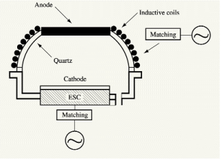
Fig1
In all commercial HDP CVD equipment in current use, there is no heating element in the deposition reactor. Wafer heating is normally initiated with an Ar plasma after the wafer is loaded into the reaction chamber. After the wafer reaches the desirable temperature, which is normally in the 300- 400°C range, other reactant gases are introduced to produce film deposition. Depending on the configuration of the plasma reactor and the type of wafer used, many process parameter sequences can be modified during deposition to minimize both electrical and physical damage to the topography and electronic features on the wafer , especially on the step corner of depositing surface features. Since production is normally implemented in a batch of 25 wafers, the argon plasma is sometimes kept on constantly between runs to maintain a baseline temperature in the deposition reactor. For both silicon oxide and fluorinated silicon oxide gap-fill film-deposition processes, a gradual ramping up of rf bias minimizes physical and electrical damage. Furthermore, gradual ramping up will reduce an initial rf power surge during the initial transient phenomena of plasma-enhanced CVD processing that may also cause unexpected damage to devices. For deposition processes, involving volatile etching reactants such as fluorines, as in the case of fluorine-doped oxide film deposition, the etching component of the HDP CVD gap-fill process becomes significant, and the rf biasing power must be reduced, compared to the case for undoped silicon oxide, in order to prevent step corner erosion.
Complex multilevel 0.20-0.25-µm STI, GC, and IMD structures with high aspect ratios (1.5-3.5) were filled with HDP CVD undoped silicon oxide. In the case of IMD structures, lower dc fluorinated silicon oxide films were also used for the gap-fill deposition. These structures were subsequently processed to several metal levels and then evaluated for dielectric gap fill, CMP integration, and plasma damage on 80-100-Å gate-oxide devices. The results were compared to those for the same device structures processed with conventional LPCVD SiO2 or plasma CVD oxide gap-fill processing.
上一篇: 氧化铝薄膜用于硅片表面钝化
下一篇: 硅片蚀刻MACE过程中化学镀金的优化