Deep etching of silicon (Si) is very much desirable for wide variety of applications. Under the context, a cost effffective and reproducible through etching of ∼375 μm thick Si wafer is demonstrated through long hour metal assisted chemical etching (MACE) followed by short duration KOH etching. During MACE, apart from pH and temperature, metal catalyst size and coverage density during electroless plating plays an important role. Optimization of gold deposition in terms of plating solution concentration and deposition time during MACE is studied for effffective through etching. HAuCl4 concentration of ∼5 mM for 30 s is found to be best suited for MACE and produces deep and highly dense pores in Si with threshold pore radius ∼250 nm and above. Following the MACE, KOH etching effffectively scoops out porous Si to realize through etching.
Deep etching of Si by wet method requires hard mask or metal as catalyst. Fabrication of through wafer micro funnel has been reported previously . Dry etching in combination with anisotropic KOH etching is adopted for realization of high density devices and interconnects in packaging. Recently, MACE based deep etching of Si is reported, where metal is deposited by evaporation or sputtering technique. Implementation of these processes in large-scale manufacturing increase the production cost. Thus, a simpler and a cost effffective method entirely based on wet synthesis is required for deep or through etching of Si wafer, resulting in large scale production of devices.
In the present work we report through etching of Si wafer using electroless plated Au as catalyst and polymer as mask. Long hour MACE is adopted to make deep and high density pores in Si, followed by short duration KOH etching to scoop out porous Si and reveal effffective etch depth. Gold electroless plating concentration and deposition time is optimized to get highly porous Si during MACE having threshold pore radius and good coverage. The fabricated through hole in Si wafer can be used as window in analysis of optical detector with out of plane contacts , through wafer interconnects and is best suited for high density device fabrication.
Fig. 1 shows SEM image of Au deposited on Si by electroless plating for 30 s in various concentration of 0.1, 1, 5 & 10 mM Au precursor. For sample (A, 30), clusters of Au nanoparticles with very low coverage density are formed, as shown in Fig. 1a. The inset of the fifigure shows initial growth of nanoparticle and seed growth during the cluster formation. With increase in metal precursor concentration for sample (B, 30), agglomeration of clusters takes place forming Au islands, and metal coverage density on substrate increases. The inset of sample (B, 30) shows the growth of highly porous interconnecting network, tending to form fifilm. For sample (C, 30) and sample (D, 30), formation of Au fifilm is observed. Inset of respective fifigures shows that the fifilm formed in sample (C, 30) is more porous with wider cracks as compared to fifilm formed in sample (D, 30).

Fig3a
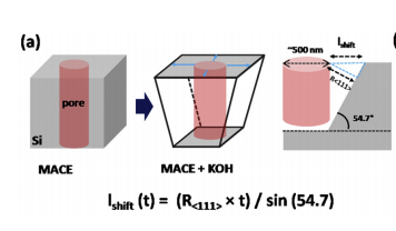
Fig. 3 shows change in morphology of single MACE etch pore after short duration of KOH etching and their evolution by merging with adjacent pores forming a larger pore. MACE of sample (C, 30) leads to formation of pores above threshold radius. The short KOH treatment widens the pore and will terminates at < 111 > facet making an angle ∼54.7° with < 100 > plane . The lateral widening (lshift) of the pore by KOH etching for time (t) min can be calculated using the formula given in Fig. 3a. The etch rates of the Si < 111 > plane (R < 111 > ) in 30 wt% KOH at 70 °C is ∼5 nm/min . For 15 min of KOH etching the calculated lateral shift is ∼90 nm. For MACE etched pores having inter-pore distance ∼180 nm, pore walls collapse after KOH treatment and they merge to form a bigger pore, as shown in Fig. 3b. Pores formed after KOH etching has straight edges due to anisotropic etching of Si.
Deep etching of Si wafer is studied with combination of MACE and KOH etching. Electroless plating of Au in various molar concentrations is adopted for MACE etching of Si wafer. Etch depth is analysed in terms of metal coverage density using stylus profifiler. High metal coverage density, results in formation of deep, wide and high density pores in Si wafer. Gold deposition in molar concentration ∼5 mM and deposition time ∼30 s is best suited for through etching of Si wafer.