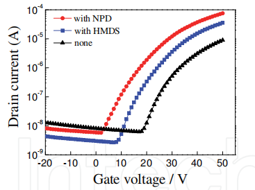
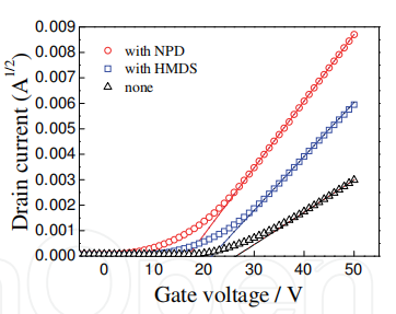
In recent years, organic transistors have attracted much attention due to their advantages in developing low-cost, flexible, and large-area production. So far, many kinds of organic materials have been reported to achieve high-performance organic field-effect transistors (OFETs). There are two types of organic semiconductors, p-type and n-type, whose majority carriers are holes and electrons, respectively. For logic gates application, both types and similar performance OFETs are required for CMOS application. Pentacene is the most popular material in p-type OFET, and many kinds of polymer materials are also reported (McCulloch et al., 2006). On the other hand, the performance of n-type OFETs is generally inferior to that of p-type (Dimitrakopoulos and Malenfant, 2002). In particular, stability in air is the most serious problem in n-type OFET. Fullerene is the most standard n-type material showing the highest mobility (Singh et al., 2007); however, the device cannot operate in air.
There are two guidelines to achieve high mobility and high stability in n-type OFET. One is to develop a new material having deeper LUMO level. Oxygen and water deteriorate OFET performance by accepting electrons from the semiconductor molecule. Therefore, enough deep LUMO level is an efficient way to avoid effect of oxygen or water. In fact, there have been many materials having deep LUMO levels, for example, perylene bisimide compound, fullerene derivatives, fluorinated compounds, and so on.
The other important point is surface treatment of the insulator. The field-effect mobility of the organic semiconductor is strongly affected by the device fabrication process. Various methods on surface treatments have been reported to improve the carrier mobility. The HMDS treatment is a standard and efficient way to make the surface hydrophobic (Lin et al., 1997; Lim et al., 2005). Organic semiconductor can aggregate with high crystallinity on the hydrophobic surface without influence of the substrate surface. These methods were developed in p-type OFETs; however, they are also efficient to improve the mobility and stability of n-type OFETs. Recently, it has been pointed out that low mobility and instability in air of n-type organic semiconductor is attributed to the surface electron traps of the gate insulator, and if electron traps can be perfectly eliminated, almost organic semiconductors can be operate in n-type mode (Chua et al., 2005). Therefore, it has been believed that the gate insulator surface should be as possible as inert to achieve high mobility and stability in n-type OFETs.
The proposed hetero-layered OFET showed improvement of the mobility compared to the conventional surface treatment. In addition, we found that the stability in air was drastically improved in n-type OFET by using a hole transporting material having higher HOMO level. We discuss the relationship between the OFET performance and the electronic property of the interfacial layer.


Fig1
These results indicate that an electronically active material can be used to fabricate an interfacial layer, and high performance can be achieved without a surface treatment of selfassembly monolayer. We also investigated some other organic materials, n-hexatriacontane that is perfectly inert material, and Alq3 that is a well-known emissive and electron transporting material. In these cases, the mobility was rather reduced to be 10-3 cm2/Vs. These results enable us to conclude that hole transporting materials are responsible for enhancing mobility.
In this section, the concept of hetero-layered OFET is applied to the combination of C60 channel layer and hole transporting material (Fig. 6). C60 is the most standard material of ntype organic semiconductors and the highest performance in n-type OFET has been reported. The device structure is the same structure with the previous section. For the interfacial layer, typical hole transporting material of NPD and m-MTDATA were used.
下一篇: OLED模块的电气和热分析