The goal of this article is to study the etching properties as a function of various adsorbed surfactant thickness in wet anisotropic etching process of TMAH solution. The thickness of preferentially adsorbed surfactant molecules on Si{110} and Si{100} has been evaluated by using spectroscopic ellipsometry (SE). The dependence of the etch rate in TMAH and the surface roughness on the layer thickness demonstrates that the surfactant is adsorbed at the interface during etching in TMAH+Triton. A thin pre-adsorbed layer is sufficient to dramatically improve the etching characteristics of silicon.
Wet anisotropic etching, regarded as a useful technology in MicroElectroMechanical Systems (MEMS), attracts researchers focusing on this field because of the inexpensive method supply and ability generating well-defined structures . Nowadays, potassium hydroxide (KOH) and tetramethylammonium hydroxide (TMAH) are the most commonly used anisotropic etchants. Based on the ability to withstand the chemical attack by these etchants, silicon oxide (SiO2), silicon nitride (Si3N4), and other metal layers (e.g. Cr, Au) have been used as masking materials. Complementary metal-oxide semiconductor (CMOS) compatibility of the anisotropic etchants is a very important issue, especially in the case of post CMOS etching, but KOH is incompatible with CMOS processing due to the presence of an alkali metal, although KOH is easy to use, non-toxic, provides excellent etching profiles and has a good selectivity between Si and Si3N4. In the etch rate TMAH is lower, but it has outstanding characteristics, such as a high selectivity between Si and SiO2, and the absence of harmful ions. Hence, TMAH solutions with and without additives are preferred in recent research and production.
Spectroscopic Ellipsometry (SE) has been utilized as a surface-sensitive technique in order to determine the thickness of thin films adsorbed on different surfaces. It is useful for probing the thickness of thin, adsorbed films on surfaces at the sub-nanometer scale.
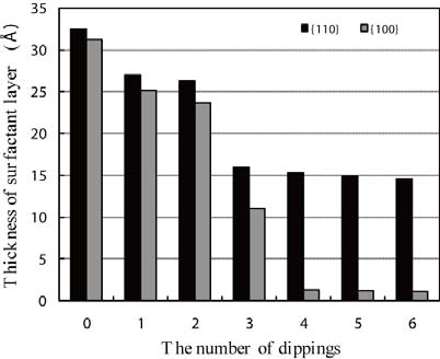
The number of dippings in DI water after the surfactant bath may affect the thickness of the adsorbed layer. Therefore, the effect of the number of gentle dippings is also studied. Moreover, the effect of ultrasonic agitation during the surfactant bath is also investigated. Bare silicon samples are used as reference surfaces.

Fig1
Ellipsometry measurements are carried out in order to characterize the formation of adsorbed layers of Triton X-100 surfactant on different surface orientations of crystalline silicon in water solutions as a function of the residence time, temperature, ultrasonic agitation and the number of dippings in DI water after residence –which can remove the most salient surfactant molecules and thus homogenize the surfactant layer. The etched surface morphology, surface roughness and etch rate are studied as a function of the surfactant layer thickness. The characteristics of surfactant thickness on {110} and {100} silicon surface and its effect in etching process can be explained as follows.