Using Au-Si eutectic bonding, devices were encapsulated by bonding a silicon cap wafer to a device wafer. Au-Si eutectic bond rings melt at over 363 ºC allowing them to conform over topology such as electrical feed-throughs allowing for a vacuum seal. Detailed specifications are given for achieving uniform/strong bonds to poly-Si and Au bond rings in a bond recipe which includes vacuum pumping, an outgassing step, application of the bond pressure (~2.5 MPa), and heating to 390 °C. Micromachined poly-Si Pirani vacuum sensors were developed, characterized and then packaged in the Au-Si eutectic bonding process in order to measuring vacuum pressures. These packages had cavity dimensions of 2.3×2.3 mm wide with a depth of 90 µm. Yields of 84.6% and 94.1% were achieved in packages with bond ring widths of 100 and 150 µm. With the use of getters and a pre-bond outgassing step, pressures from <3.7 to 23.3 mTorr were achieved. Furthermore, pressures were shown to remain stable to within ±5 mTorr for over 3 years of testing, after 100 hours at 150ºC, and after 50 thermal cycles from -50ºC to 150ºC.
Using differential localized heating, one of the two wafers to be bonded is heated from the backside, and the other is cooled from the backside, so that heat flows through the bond regions while the device regions stay relatively cool. A bonder test setup was built where integrated temperature sensors on the device wafer were used to measure the temperature at different distances from the bond region during Si to glass and Si to Si bond experiments. This technique was proven successful with temperature of 23% and 41% of the bond ring temperature at 250 and 650 µm from the bond rings for bonds to glass and Si respectively. These temperature rises were within 3% and 9% of those predicted by 3-D FEM thermal modeling. In the Si to glass bond, bond rings were heated to 400ºC allowing for a Au-Si eutectic bond.
Only 7 years after the invention of the transistor in 1947, Texas Instruments was selling silicon transistors and by the early 1960’s the first computers were made using circuits with small scale integration. Now integrated circuits (ICs) are an integral part of nearly all of the electronics that we use and the semiconductor industry has turned into a $200 billion/year market. In contrast, the first microelectromechanical systems (MEMS) pressure sensors were not commercially available until the 1980s and it was not until the 1990s that MEMS accelerometers were mass produced for automotive crash detection and that Texas Instruments brought DMD (digital micro-mirror devices) to market for projection displays. Despite the fact that MEMS technology is based on the same fabrication and lithographic techniques used for the production of ICs, the commercialization of MEMS devices has lagged behind. One reason for this longer gestation period is the added complexity in packaging MEMS devices which either prevents their commercialization or significantly adds to the cost of manufacturing. Furthermore, packaging often accounts for greater than 50% of the total cost of manufacturing a MEMS device .
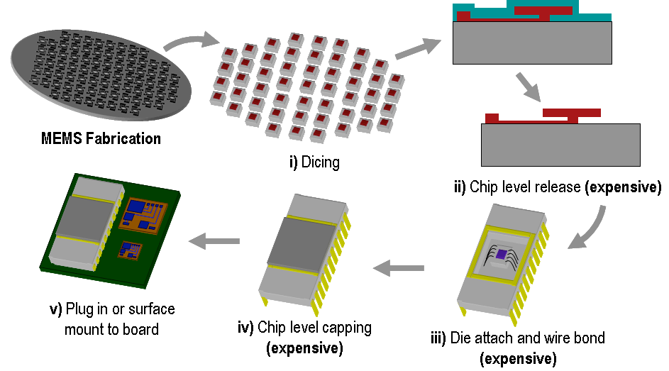
Many of the same thermal management and interconnection issues involved in IC packaging also apply to the packaging of MEMS with a whole set of additional challenges. These packaged parts in fact have micro- and nanometer dimension that need to interact with the environment for sensing but need protection from even the smallest particles. Although no one package design is suitable for all applications, in general there are two tracks for packaging MEMS devices: chip-level packaging and wafer-level packaging. Figure 1.2 shows a typical chip-level packaging sequence in which: i) the device is first diced (sawed from the wafer it was fabricated on), ii) the device is released (etching a film away so that the moving part can move), iii) the device is encapsulated in a dual-in-line (DIP) package or using flip chip in package (FCiP) technology, and iv) the DIP or FCiP is plugged in or soldered onto a PCB to interact with drive circuitry or other components. As labeled in Figure 1.2, steps ii) through iv) are costly because they are done serially on one device at a time. Also, because steps ii) through iv) involve the handling of un-capped micro-mechanical parts, this approach often results in reliability issues and yield loss.

Fig1.2
Figure 1.3 shows a process sequence for the wafer-level packaging approach where devices: i) are released at the wafer-level, ii) encapsulated (using either another wafer or a thin film) while they are still on the wafer, iii) diced, and iv) the package is wirebonded or flip chipped directly onto the PCB to interact with drive circuitry or other components. In the wafer-level approach all of the devices are released and encapsulated at once (in steps i) and ii)) on the wafer—thus reducing cost. In addition, these processes are done in a clean room environment which potentially increases their reliability. Furthermore, the wafer-level approach reduces overall package size which can help to further reduce the cost of manufacturing.
上一篇: 声电化学参数在半导体清洁中的作用
下一篇: 多层衍射光栅清洗方法的评价