This article presents a set of low-temperature deposition and etching processes for the integration of electrochemically deposited Ni-Fe alloys in complex magnetic microelectromechanical systems, as Ni-Fe is known to suffer from detrimental stress development when subjected to excessive thermal loads. A selective etch process is reported which enables the copper seed layer used for electrodeposition to be removed while preserving the integrity of Ni-Fe. In addition, a low temperature deposition and surface micromachining process is presented in which silicon dioxide and silicon nitride are used, respectively, as sacrifificial material and structural dielectric. The sacrifificial layer can be patterned and removed by wet buffered oxide etch or vapour HF etching. The reported methods limit the thermal budget and minimise the stress development in Ni-Fe. This combination of techniques represents an advance towards the reliable integration of Ni-Fe components in complex surface micromachined magnetic MEMS.
Electrochemically deposited alloys of nickel and iron (ECD Ni-Fe) are attractive materials for the fabrication of integrated magnetic microelectromechanical systems (MEMS) . Although highly desirable for their large magnetic permeability and low coercivity , ECD Ni-Fe alloys are known to suffer from chemical deterioration when exposed to subsequent processing steps and require therefore careful planning during the process integration stage.
Electroplating requires the preliminary deposition of a conductive seed layer that serves as a nucleation surface for the growth of the desired material through patterned moulds. Copper is one of the most commonly used seed layer materials, as it offers a balance between high conductivity, thus reducing non-uniformities caused by radial voltage drops on the wafer during electrodeposition, and ease of processing . After electrodeposition, the mould is stripped and the exposed seed layer must be removed to electrically isolate the individual electroplated structures. To this end, wet etch processes are preferred to dry etching as the latter require expensive tools and possibly further masking. Conventional copper wet etchants are solutions based on (NH4)2S2O8, HNO3, HCl/CuCl2 or HCl/FeCl3. None of these chemicals is, however, selective enough to enable the copper to be removed while leaving Ni-Fe intact . A method to selectively wet etch copper in the presence of structural ECD Ni-Fe elements using conventional etchants is therefore desirable to facilitate the integration of soft magnetic elements in complex process flflows while still employing standard techniques.
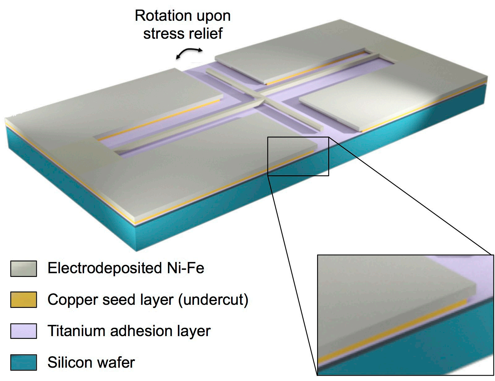
A conceptual drawing of the test structures used for this investigation is shown in Figure 1. Rotating structures of this kind are typically used as strain sensors, but they can also indicate the completion of the etch release process.

Fig1
At this stage, the copper seed layer is etched (Figure 2f). The exposed copper surface is etchedfirst, followed by the undercut underneath the Ni-Fe structures. Once the undercut etch is sufficient tocompletely remove the copper undernea th the narrow beams (4 um sideways etch) , these are no longeibound to the substrate and free to contract or expand to relieve the residual stress. The observatiorof a movement of the pointer arm is therefore an indication of the completion of the copper etchunderneath the beams. The larger electrodeposited areas of the anchor pads at this stage remain fullanchored to the substrate, as the undercut only extends to half the width (4 um) of the narrow Ni-Fbeams, plus any over-etch.
To verify the effectiveness as complexing agent, 50 gL-I of citric acid were dissolved in the etchantto prevent the reduction of copper on Ni-Fe. The new etching solution was tested on another waferand the results are presented in Figure 6. The undesired effects of Ni-Fe corrosion and redepositionof etched metal are eliminated and the copper seed layer is completely removed after 3-5 min in theetchant. as indicated by the rotation of the pointer arms and the clean wafer surface, which appearsfree of residue.
上一篇: 多孔硅的导热率、光导率和电导率的变化
下一篇: 硅通孔的湿法工艺技术