After many years as a hypothetical possibility, 3D IC stacking has emerged as a potential key enabler for maintaining semiconductor performance trends. Implementing 3D, however, will almost certainly require development of throughsilicon vias (TSVs), which in the past few years have been elevated by the semiconductor industry to the status of a crucial mainstream technology.
Producing these vertical connections can seem misleadingly straightforward: drill a blind hole through the silicon wafer, deposit a uniform liner layer of dielectric material to electrically isolate the via, deposit a barrier layer to prevent copper from diffusing into silicon, and then completely fill the via with electro-chemically deposited (ECD) copper. An additional copper-seed layer may be needed before via filling if the selected barrier material is too resistive to allow the inception of the ECD process; as we will see, this is the case for most dry-process barriers, but not for all barrier materials. CMP and wafer-thinning steps conclude the sequence.
Electrografting deposition of a Cu seed layer, using a bath containing specific organics and copper, is also available, and has already been described. It has been shown how an electrochemical process is applied to provide a conformal and continuous copper seed layer directly on various dry and wet barriers. It has already been proven that electrografting Cu seed layers meet or exceed all TSV requirements. For the remainder of this paper, we will focus on electrografting isolation and chemical grafting barrier.
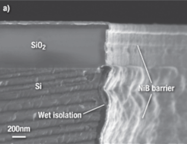
A single-step wet deposition method has been developed for nickel-based barriers on eG isolation and dry dielectric layers (such as SiO2, SiC, SiOC or SiN). This approach enables a cost-effective, streamlined process for via-middle and via-last applications, where TSVs are drilled through a stack of different materials. An example of one-step barrier deposition over eG isolation/SiO2 is shown in Fig. 1a.

Fig1(a)
Film thickness can be controlled to any value from 40 to 400nm with maximum nonuniformity of 5% 3σ in-wafer (300mm). This provides a step coverage value (bottom/top thickness ratio) of up to 90% for liner and metal layers. As a reference, typical dry-process barrier step coverage values are below 10% for 10:1 aspect ratio TSVs. Adhesion of all layers was measured using a 16-squares scribe tape test method: all layers successfully passed the test. Film properties for each layer, as well as reliability test results, are discussed in detail in [1]. Selected basic film properties are summarized in Table 1. Barrier properties have already been described in [9] and proved to be equivalent to industry reference barriers.
underlying layer. As noted earlier, this is the reason Cu-seed layers are required. However, because of the extremely poor step coverage of dry-process barrier and seed layers (<10%), sheet resistance values at the bottom of the via are very high, making it difficult to initiate the filling process. As a reference, current strongly acidic chemistries require Rs values smaller than 0.2Ω/sq, which converts to a minimum of 100nm thickness for the Cu seed layer.